能源管理的小型便携式系统-Energy Management
Numerous diverse and conflicting constraints burden the designer of small hand-held products. Aside from the customary restrictions on size and weight, these constraints include cost limitations, strict time schedules, battery-life goals measured in weeks instead of hours, and host computers that are (sometimes) overtaxed with the demands of power management.
Because power requirements for hand-held applications vary widely with product use, no single "best" power source exists for these applications. A device used intermittently is more concerned with no-load quiescent current than with full-load efficiency, and so may operate satisfactorily with alkaline batteries. Cell phones, on the other hand, must contend with high peak loads and frequent use. This mode of operation emphasizes conversion efficiency over quiescent current, so cell phones are better served with a rechargeable battery.
In hand-held product design, size limitations often dictate the number of battery cells early in the process. This is frustrating to the electrical engineer, and a substantial constraint, since the number (and type) of cells allowed determines the operating-voltage range, which in turn strongly affects the cost and complexity of the power supply. High cell counts enable the use of linear regulators and simple circuitry at the cost of extra weight and limited efficiency. Low cell counts compel the use of a more costly switching regulator, but the low cost of the battery may justify this expense.
Four-Cell Designs
Four-cell batteries often provide an attractive compromise between weight and operating life. That number is particularly popular for alkaline batteries because they are commonly sold in multiples of four. Four-cell power for 5V circuitry presents a design challenge, however. As the battery discharges, the regulator must first step down, and then step up. This requirement precludes use of the simpler, one-function regulator topologies that can only step down, step up, or invert.
One effective solution to this problem is the SEPIC (single-ended primary inductance converter), in which VOUT is capacitively coupled to the switching circuitry (Figure 1). The absence of a transformer is one of several advantages this configuration has over flyback-transformer regulators and combination step-up/linear regulators.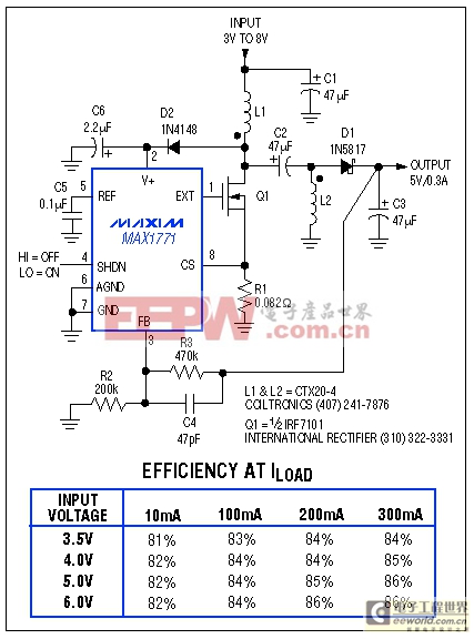
Figure 1. This regulator topology supplies 5V for inputs ranging from 3V to 8V. The operation shifts smoothly between step-up and step-down conversion without steps or mode changes. During shutdown, the output turns off completely and sources no current.
As another improvement over boost designs (in which current drains from the battery during shutdown unless you add a cut-off switch—see (Figure 2), the SEPIC output fully turns off in response to a shutdown command. As VIN falls during normal operation, the SEPIC circuit smoothly regulates VOUT without shifting its mode of operation as VOUT approaches VIN. Its power-conversion efficiency peaks at 86%, near 200mA (Figure 1).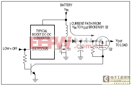
Figure 2. Typical dc-dc boost converters provide a current path from input to output, even when powered down. To interrupt this path, you must add a disconnect switch (Q2).
Coils L1 and L2 (Figure 1) should be the same type and have the same value, but coupling between them is not required. They can be wound on the same core for convenience, but the circuit works equally well if they are completely separate. Each coil passes only one half of the peak switching current (IPEAK = 100mV/R1 = 1.22A), so each can be rated accordingly.
Capacitor C2 couples energy to the output and requires low ESR to handle high ripple currents. A low-ESR Sanyo OS-CON capacitor, for instance, offers 3% more efficiency than does a less expensive 1μF ceramic capacitor. Tantalum capacitors are not recommended because high ESR causes them to self-heat at high ripple currents.
Diode D2 provides a supply voltage for the IC (pin 2) by capturing switching pulses at the drain of Q1. Although this voltage (approximately the sum of VIN and VOUT) limits the maximum VIN to 8V, it improves the start-up capability under full load and improves the low-VIN efficiency by boosting gate drive to the external MOSFET. If VIN does not fall below 4V, you can substitute a 3V-threshold FET for Q1 and omit D2. In that case, pin 2 connects directly to VIN, which assumes an upper limit of 16.5V.
模拟电源 电源管理 模拟器件 模拟电子 模拟 模拟电路 模拟芯片 德州仪器 放大器 ADI 相关文章:
- 采用数字电源还是模拟电源?(01-17)
- 模拟电源管理与数字电源管理(02-05)
- 数字电源正在超越模拟电源(03-19)
- 数字电源PK模拟电源(04-03)
- TI工程师现身说法:采用数字电源还是模拟电源?(10-10)
- 开关电源与模拟电源的分别(05-08)