能源管理的小型便携式系统-Energy Management
designers would regard the ideal converter circuit as one that has no inductor. The capacitor-based alternatives (charge-pump converters) were hampered in the past by their lack of regulation and limited output current. Though still low compared to that of switching regulators, their output current is now adequate for many designs. And in some cases, the charge-pump advantages are compelling—low cost, small size, and reduced EMI. Charge pumps are particularly useful in PCMCIA systems and other "credit-card" products in which the component height is limited.
Figures 8, 9, and 10 illustrate three inductorless voltage converters. In Figure 8, the output of a 2-cell battery or other low-voltage source is converted to a regulated 5V ±4%. The IC changes its operational mode with input voltage, producing a tripler at low VIN, a doubler at high VIN, and a tripler-doubler at mid-range that changes modes every switching cycle. Efficiency ranges from 85% to 65%. Low supply current—typically 75μA for no-load operating conditions and 1μA in shutdown—makes the circuit useful as a coin-cell-powered backup supply for DRAM or PSRAM.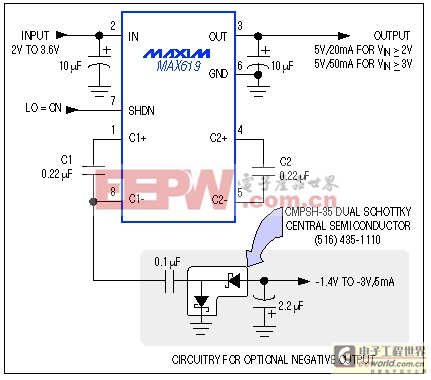
Figure 8. With a few external capacitors, one IC boosts a 2-cell or 3-cell input to 5V, and delivers 50mA (for 3V inputs) with only 75μA of quiescent current. With an additional SOT-23 dual diode and two capacitors, it also produces a small negative output.
The optional diode-capacitor network in Figure 8 generates an unregulated negative voltage between -1.4V and -3V. Acting as a negative supply, this output simplifies analog designs by allowing the use of inexpensive op amps. The negative rail assures that such op amps can swing completely to ground.
Another charge-pump circuit, built in less than 0.1in.2 of board area, converts 5V to the 12V level required for programming "flash" memory chips (Figure 9). Common in PCMCIA cards, flash memory is popular for compact portable applications because it provides large amounts of nonvolatile storage in a small space, and because it needs power only for read and write operations. Some flash ICs operate on 5V, but those with the highest memory densities require 12V for programming.
Figure 9. For programming flash memory, this circuit generates a regulated 12V/30mA programming voltage without inductors. It's small enough to fit into "smart cards" the size of a credit card.
A third application that benefits from the use of charge pumps is the optimization of RF-transmitter efficiency in cellular and other voice/data wireless transceivers. "Talk time" in these transceivers is extended by the use of power amplifiers based on gallium-arsenide FETs (GaAsFETs), which are more efficient than those based on bipolar transistors.
Though more efficient, a GaAsFET costs more and requires a small negative bias voltage. Typical charge pumps generate too much noise for this application, but an output voltage regulator in the chip of Figure 10 holds the output noise and ripple to 1mVp-p. Tying the FB terminal to ground sets the regulated output to -4.1V (you can set other output levels with two external resistors). Regulation and low noise are achieved with an output linear regulator—unlike the circuits of Figures 8 and 9, which regulate by gating the charge pump's switching action.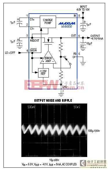
Figure 10. Intended for biasing efficient GaAsFET RF power amplifiers, this charge-pump voltage inverter includes a super-quiet linear regulator that limits output ripple and noise below 1mVp-p.
Intermittent High-Current Loads
A second requirement in many hand-held wireless designs is a quick response to ab
模拟电源 电源管理 模拟器件 模拟电子 模拟 模拟电路 模拟芯片 德州仪器 放大器 ADI 相关文章:
- 采用数字电源还是模拟电源?(01-17)
- 模拟电源管理与数字电源管理(02-05)
- 数字电源正在超越模拟电源(03-19)
- 数字电源PK模拟电源(04-03)
- TI工程师现身说法:采用数字电源还是模拟电源?(10-10)
- 开关电源与模拟电源的分别(05-08)