What is wrong with this emmmiter follower?
Which emetter follower ur telling About? the final stage ur implimenting is not an emitter follower...
pls find the attached image....[IMG]
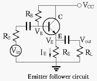
sorry its a buffer amplifier
Check or tweak R4 R5 resistors, if possible place another resistor between node 6 and Q2.
In my view emitter follower is buffer amplifier
emitter follower is a unity gain amplifier which is also called buffer Ampr.
I think there's a good clue in the other Voltages displayed.
The peak-peak voltage at the emitter of the oscillator is 5.19v and at the emitter of the buffer is 5.15v. That would appear to be correct, only a slight loss.
But the RMS voltage has dropped greatly. This implies that the waveform is severely distorted. I think it would be very apparent on a real-time 'scope! We could expect that distortion to be a consequence of transistor's non-linearity or a consequence of your DC offsets. In this circuit, I guess its the worryingly low DC voltage on the oscillator's emitter.
If so, then you need to adjust the DC biasing of the oscillator to get that 5 volt waveform nicely centred between the 0 v and 9 v power rails. That might take you some time because it doesn't leave you a lot of voltage left, but I'm sure you'll manage.
DC bias is controlled by R4,R5, R6 and suggested res between node 6 and Q2.
I understood that a resistor between +9 and the collector also was your advice in your earlier post. However any resistance in the collector current of the output buffer will simply reduce the amplitude further, which is the opposite effect from what the OP is seeking.
But you are of course quite correct that the bias of that output transistor is determined by R4 & R5 just as the bias of the oscillator is set by R1 and R2. Thanks to C4, the DC conditions of both halves of the circuit are isolated from each other, so may be adjusted independently.
Ok so what resistor should I change to obtain higher vrms at the collecter?
My reply to you was "If so, then you need to adjust the DC biasing of the oscillator to get that 5 volt waveform nicely centred between the 0 v and 9 v power rails. That might take you some time because it doesn't leave you a lot of voltage left, but I'm sure you'll manage.". I was trying to suggest that you could use an oscilloscope to look at the signal on the emitter of both transistors.
Firstly, you might be able to confirm if my analysis was correct. (Or not).
Secondly, you would see whether the distortion was apparent after the oscillator or only after the 'emitter follower'. (On one, or the other, or both, or neither).
Thirdly, what you observe might guide you to making an appropriate adjustment.
Fourthly, I was suggesting that it might take some time re-iterating a few adjustments to get the result you want.
But here we are, miles away. I can't see your 'scope, I don't know where the distortion is being developed. I can't see how badly underbiased (or overbiased) either transitor(s) is/are, but you'd still like me to suggest a resistor value! Ok. I'll make some guesses if that's how you want to do this.
So my guess in the dark is . . . . . its Q2 that is introducing the distortion and that it is overbiased. So change R4 from 15k to 47k and change R5 from 15k to 100k.
Or you could calculate the bias current for a BC548B and come up with the correct answers!