impedance matching going the wrong way
As I change the matching components and read the impedance, the readings I get are very different from what I would have expected.
I'm measuring at 905MHz and the impedance seems to be moving sideways. If anybody has any pointers I sure would like to hear them.


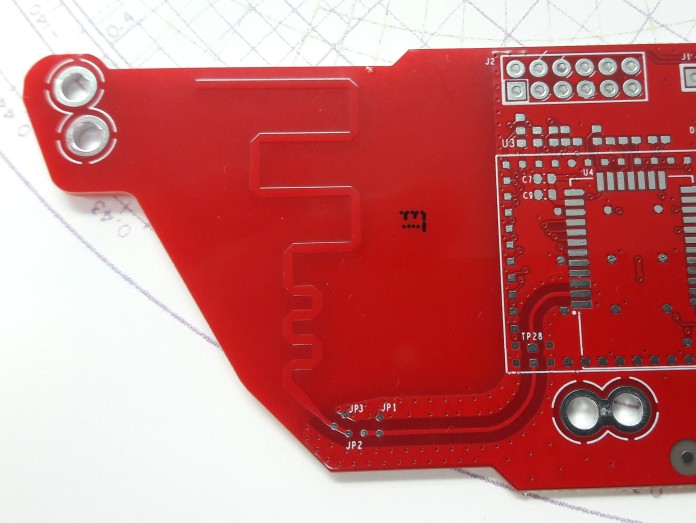
J1, closest to source, parallel component
J2, middle, series component
J3, closest to antenna, parallel component
point 1: starting without matching, using 0-ohm jumper at J2.
point 2: added 4.7pF at J3 (parallel)
point 3: decreased from 4.7 to 1pF
point 4: increased from 1 to 3.3pF
observing impedance moving sideways instead of down.
point 5: added 2.2nH at J2 (series)
point 6: increased 2.2 to 3.6nH
point 7: increased 3.6 to 6.2nH
observing further sideways movement
point 8: added 12nH at J1 (parallel)
point 9: increased from 12 to 22nH
point 10: replace J2 6.2nH with 0-ohm jumper (series).
Because you're using wrong side of Smith Chart.
What is your impedance and frequency ?
I'm not motivated to reproduce the calculation without a matching network schematic.
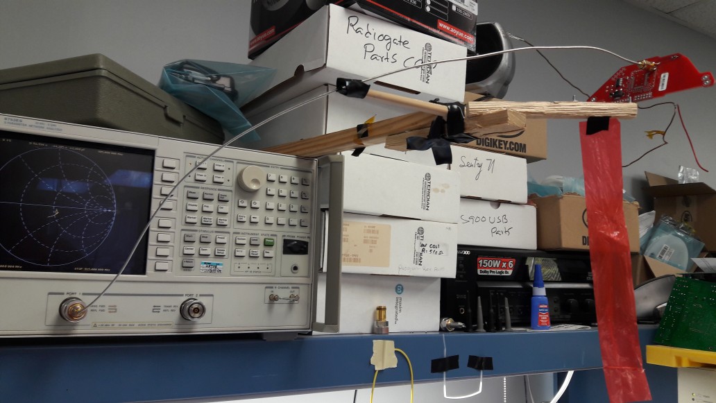
Besides possibly wrong calculation, I don't believe that the measurement setup can ever give realistic impedance values without thorough isolation of the feed line, e.g. using ferrite tubes.
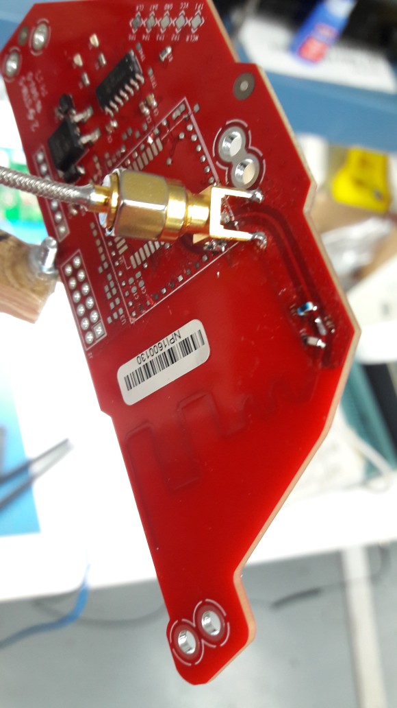
Yes, most seems wrong. Measured phase seems wrong and measurement setup could be better. Use ferrite tubes to avoid adding vna cable as part of the ground and if possible avoid that SMA arrangement at PCB.
Simplest, cut cable near end, add ferrite tubes, solder cable braid directly at PCB after remove paint at ground so that it is possible to make real good contact to braid near actual test point.
Probably biggest mistake to avoid in this case, before soldering center cable to PCB, verify that phase delay at VNA shows as a dot 3 o'clock at Smith chart when when unconnected and a shortcut should be seen as a dot 9 o'clock.
If not, adjust port forwarding or electrical delay for correct phase. If losses are high in measurement cable so that these points not can be reached, do a SOL calibration directly at PCB by using existing pads for matching network as calibration points.
Forgot, after measurement cable is soldered at test point, do a temporary shortcut at location for tuning components and calibrate vna port delay for this location.
impedance matching wrong 相关文章:
- Output Impedance Of a Triple cascode
- How to make image impedance equal
- Input and output impedance matching in Distributed amplifier
- Characteristic impedance of combination of CPWG and stripline on inner layers
- Problem of impedance matching of Gilbert cell mixer
- Input impedance of transmission lines connected in cascade
