What is wrong with the insertion loss of HMC347
Figure 1 Schematic of HMC347
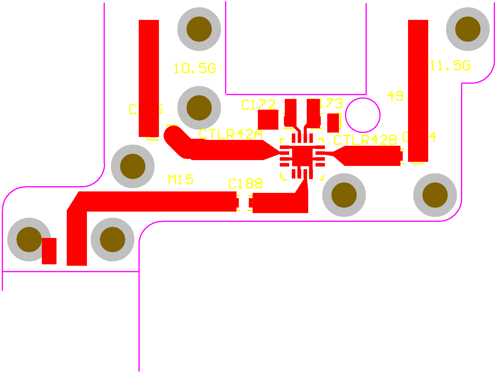
and part of pcb is as follows (according to the ic designator U22 ):
Figure 2 part of pcb (U22)
The board material is RO4350B, with effective dielectric const of 3.48, and the 50 Ohm character resistance width is about 1.74mm. The ac-coupled capacitors are from ATC.
However, when I test the pcb in Fig.2 separately, I found the insertion loss is about 1.7dB for 8GHz, and about6dB for 10GHz, about 12dB for 12GHz, which is terrible for I used 4 switches, which would cause about 48dB loss for 12GHz. The loss of connector and test coaxes is subtracted. Referring to the isolation, which is only about 10dB for 12GHz.
What is wrong with the circuit? Can I achieve the parameters in the datasheet? or something is hided in the datasheet? What is the measuring method of datasheet parameters? The attachment is the datasheet of HMC347LP3. Any reply is appreciated. Thank you!

Have you connected all the grounds properly to PCB ground, as short as possible?
Ground for microstrip lines is on PCB backside, and I don't see any vias at the switch pads?

Beside possible missing ground vias, I fear that the relative thick substrate (0.8 mm or so) and respective wide 50 ohm traces will cause considerable discontinuities in the 10 GHz range. You should check the effective series inductance of coupling capacitors and tapered micro strip end segments.
I am sorry, the vias in the ground pad plane accordingly are 4 with 0.18 mm width, which are not displayed in the fig2. Actually there are ground vias below the ground pad.
I think you are right. But I do not see that the 0.8 mm substrate should not be used in the high frequency band in any books. If it is a fact, it will be funny.
Do you know butterfly ground?
You should treat your PCB layout very careful.
Do you simulate it, the bend, etc?
If not, you should not be weird.
There's no principle reason not to use 0.8 mm substrate, but many practical.
I reviewed the evaluation board drawing (unfortunately there are no exact dimensions or gerber files). It uses a coplanar strip with ground, my rough estimation is 0.4 mm line width and 0.3 mm ground separation, would require a substrate thickness in the 0.2 mm range for 50 ohm impedance.
Besides already discussed unsuitable strip line dimensions and discontinuity problems, you get relative large ground via inductance with 0.8 mm substrate. I guess that 4 vias will contribute enough series inductance to worsen the isolation performance of the absorptive switch.
0.8mm can be used at Microwave Region but discontinuities are pretty important due to di-electric coefficient that is small ( transitions between MS Lines and IC pads are a bit weird.)
In additional to, mounting holes are too close to the transmission lines and they may create a loss mechanism due to approximation effect.