求助DRC error
有一些是因为desity不够,可以在所报区域加上一些dummy来解决;我很疑惑的是,为什么encounter布局布线,还会有Metal间距的问题(第29个)和Metal宽度的问题(第25个)?其它的错误都要解决吗?谢谢指教!
1.
Spacebetween N-Well edge and an N+ AA region which is outside an NW is >= 0.43um
2.
N-Wellenclosure of a P+ AA region which inside an NW is >= 0.43um
3.
Spacebetween GATE edge and edge of a butted diffusion AA region is >= 0.32um
GT width for interconnects is >= 0.18um
4.
Spacebetween two GT regions on field oxide area is >= 0.25um
5.
Polyextension of AA is >= 0.22um
6.
Extensionfrom AA region to GT is >= 0.32um
7.
Spacebetween field interconnect poly and AA is >= 0.10um
8.
GTdensity is >= 14%
9.
Spacebetween two GTs on AA which is with CT is >= 0.375um
10.Spacebetween SN and a non-butted edge of P+ pick-up AA region is >= 0.10um
if the distance between P+ AA and N-well >= 0.43m
11.Spacebetween a SN region and a non-butted edge of P-well pick-up P+ AA region
is >= 0.18um if the distance between P+ AA andN-well < 0.43um
12.Enclosureof a SN edge to an N-channel Poly gate along source/drain direction is >=0.32um
13.Enclosureof a SN edge to a N-channel Poly gate along the direction of poly gate is >=0.35um
14.Spacefrom a SN edge to a P-channel Poly gate along the direction of poly gate is>= 0.35um
15.Spacebetween SP and a non-butted edge of N+ pick-up AA region is >= 0.10um
if the distance between N+ AA and P-well >= 0.43m
16.Spacebetween a SP region and a non-butted edge of N-well pick-up N+ AA region
is >= 0.18um if the distance between N+ AA and P-well< 0.43um
17.Enclosureof a SP edge to P-channel Poly gate along source/drain direction is >=0.32um
Space from a SP edge to a P-channel Poly gate alongthe direction of poly gate is >= 0.35um
18.Spacefrom a SP edge to a N-channel Poly gate along the direction of poly gate is>= 0.35um
19.Spacebetween poly CT to AA is >= 0.20um
20.Spacebetween poly to diffusion CT is >= 0.16um
21.Enclosureof an AA region beyond an AA CT region is >= 0.10um
Enclosure of a poly region beyond a poly CT region is>= 0.10um
22.Vnsize is = 0.26um (exclude Metal-fuse's Protection Ring area and MARKS seal ringarea).
The size should be performed on all area whichincludes the DRC block layer
23.Spacebetween two Vns is >= 0.26um
24.Vnsize is = 0.26um (exclude Metal-fuse's Protection Ring area and MARKS seal ringarea).
The size should be performed on all area whichincludes the DRC block layer
25.M1width is >= 0.23um
26.Spacebetween two M1 regions is >= 0.23um
27.Enclosureof M1 region over CT region is >= 0.005um.
Enclosure of M1 line end region beyond CT region is>= 0.06um. For CT at 90 degree corner, one side must be considered as lineend region.
28.Spacebetween M1 lines with one or both metal line width and length are greater than10um is >= 0.60um.
The minimum space must be maintained between a metalline and a small piece of metal (< 10um) that is
connected to the wide metal within 1.00um range fromthe wide metal
29.Spacebetween two Mn-1 regions is >= 0.28um
30.Minimumspace between Mn-1 lines with one or both metal line width and length aregreater than 10um is 0.60um
The minimum space must be maintained between a metalline and a small piece of metal(<10) that is connected
to the wide metal within 1.0um range from the widemetal.
31.Mn-1density is >= 30%. Dummy pattern is required for
those with Mn-1 density less than 30%
32.Spacebetween two Mn-1 regions is >= 0.28um
33.Mn-1density is >= 30%. Dummy pattern is required for
those with Mn-1 density less than 30%
34.Minimumspace between Mn-1 lines with one or both metal line width and length aregreater than 10um is 0.60um
35.Theminimum space must be maintained between a metal line and a small piece ofmetal(<10) that is connected
to the wide metal within 1.0um range from the widemetal.
36.Mn-1density is >= 30%. Dummy pattern is required for
those with Mn-1 density less than 30%
37.MTdensity is >= 30%
Dummy pattern is required for those with MT densityless than 30%
38.(Thisis for M4/M5/M6 stack)
39.Minimumspace between a small metal island and a big metal block is 1.00um.(small metalisland: width*length < 1um*um
big metal block: width > 25um, length > 100um)
40.TheBORDER layer must enclose all chip layout patterns, which all chip layoutpatterns
include seal ring if seal ring has been added bydesigners.
This rule checking includes the layers of DNW,AA,NW,MVN, MVP,DG,GT,SN,SP,SAB,CT,M1,V1,Mn,
Vn,TMn,TVn,PA,Fuse,AADUM,GTDUM,MnDUM,TMnDUM
41.Enclosureof AA, GT, CT, Mn(n=1-5), Vn(n=1-5), TM by BORDER layer if it need SMIC to add
seal ring. (AA, GT, CT, Mn, Vn, TM are OPC treatmentlayers) is >= 1.1um.
42.PMOSin PW is not allowed
没加filler吧,感觉,你列的error太多了,没人会帮你看的
首先edi里面要verifygeometry,verifyconnectivity过,
verifygeometry,verifyconnectivity确实有问题,有Antenna(Dangling Wire),open, spacing,short的问题,为什么会有这些问题呢?如下图所示,该如何着手解决Antenna(Dangling Wire),spacing的问题呢?谢谢!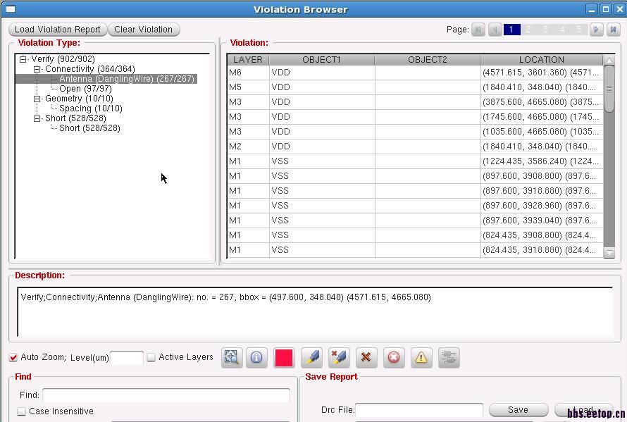
这个要有人在旁边和你说才行,讲不清,
请问这个需要手动修改还是可以在encounter里面选择一些选项就可以解决?以前流片从来不会遇到这种情况,一般encounter的时候就没有Connectivity和Geometry的问题。谢谢!