运用互补性显微术在终极尺度上三维重构并分析同一个纳米级样品
时间:04-29
来源:互联网
点击:
鸣谢
本作品投资方为RechercheTechnologique de Base (RTB)和法国国家研究局APTITUDE项目(ANR-12-NANO-0001),实验是在MINATEC的 Nanocharacterisation平台(PFNC)上完成的。
1. A. Asenov and S. Saini, Electron Devices, IEEE Transactions on 46 (8), 1718-1724 (1999).
2. P. A. Stolk, F. P. Widdershoven and D. B. M. Klaassen, Electron Devices, IEEE Transactions on 45 (9), 1960-1971 (1998).
3. S. Roy and A. Asenov, Science 309 (5733), 388-390 (2005).
4. H. Takamizawa, Y. Shimizu, K. Inoue, T. Toyama, N. Okada, M. Kato, H. Uchida, F. Yano, A. Nishida, T. Mogami and Y. Nagai, Applied Physics Letters 99 (13), - (2011).
5. T. Tsunomura, A. Nishida, F. Yano, A. T. Putra, K. Takeuchi, S. Inaba, S. Kamohara, K. Terada, T. Hiramoto and T. Mogami, presented at the VLSI Technology, 2008 Symposium on, 2008 (unpublished).
6. D. Blavette, A. Bostel, J. M. Sarrau, B. Deconihout and A. Menand, Nature 363 (6428), 432-435 (1993).
7. D. J. Larson, D. Lawrence, W. Lefebvre, D. Olson, T. J. Prosa, D. A. Reinhard, R. M. Ulfig, P. H. Clifton, J. H. Bunton, D. Lenz, J. D. Olson, L. Renaud, I. Martin and T. F. Kelly, Journal of Physics: Conference Series 326 (1), 012030 (2011).
8. h. w. i. n. International Technology Roadmap for Semiconductors 2013 Edition Design.
9. G. L. Kellogg and T. T. Tsong, Journal of Applied Physics 51 (2), 1184-1193 (1980).
10. B. Gault, F. Vurpillot, A. Vella, M. Gilbert, A. Menand, D. Blavette and B. Deconihout, Review of Scientific Instruments 77 (4), 043705-043708 (2006).
11. S. Duguay, T. Philippe, F. Cristiano and D. Blavette, Applied Physics Letters 97 (24), 242104-242103 (2010).
12. K. Inoue, F. Yano, A. Nishida, H. Takamizawa, T. Tsunomura, Y. Nagai and M. Hasegawa, Ultramicroscopy 109 (12), 1479-1484 (2009).
13. I. Koji, T. Hisashi, S. Yasuo, Y. Fumiko, T. Takeshi, N. Akio, M. Tohru, K. Katsuyuki, M. Takahiro, K. Jun, A. Seishi, O. Noriyuki, K. Mikio, U. Hiroshi and N. Yasuyoshi, Applied Physics Express 6 (4), 046502 (2013).
14. K. Ajay Kumar, K. Arul, F. Antonios and V. Wilfried, Nanotechnology 24 (27), 275705 (2013).
15. H. Takamizawa, Y. Shimizu, Y. Nozawa, T. Toyama, H. Morita, Y. Yabuuchi, M. Ogura and Y. Nagai, Applied Physics Letters 100 (9), - (2012).
16. H. Takamizawa, Y. Shimizu, K. Inoue, T. Toyama, F. Yano, A. Nishida, T. Mogami, N. Okada, M. Kato, H. Uchida, K. Kitamoto, T. Miyagi, J. Kato and Y. Nagai, Applied Physics Letters 100 (25), - (2012).
17. M. Gilbert, W. Vandervorst, S. Koelling and A. K. Kambham, Ultramicroscopy 111 (6), 530-534 (2011).
18. D. Blavette, F. Vurpillot, P. Pareige and A. Menand, Ultramicroscopy 89 (1–3), 145-153 (2001).
19. F. Vurpillot, A. Bostel and D. Blavette, Applied Physics Letters 76 (21), 3127-3129 (2000).
20. A. Grenier, S. Duguay, J. P. Barnes, R. Serra, G. Haberfehlner, D. Cooper, F. Bertin, S. Barraud, G. Audoit, L. Arnoldi, E. Cadel, A. Chabli and F. Vurpillot, Ultramicroscopy 136, 185-192 (2014).
21. M. K. Miller and M. G. Hetherington, Surface Science 246 (1–3), 442-449 (1991).
22. E. A. Marquis, B. P. Geiser, T. J. Prosa and D. J. Larson, Journal of Microscopy 241 (3), 225-233 (2011).
23. C. Oberdorfer and G. Schmitz, Microsc. microanal. 17 (01), 15-25 (2011).
24. I. Arslan, T. J. V. Yates, N. D. Browning and P. A. Midgley, Science 309 (5744), 2195-2198 (2005).
25. E. Biermans, L. Molina, K. J. Batenburg, S. Bals and G. Van Tendeloo, Nano Letters 10 (12), 5014-5019 (2010).
26. D. J. Larson, T. J. Prosa, R. M. Ulfig, B. P. Geiser and T. F. Kelly, Springer New York (2013).
27. P. Bas, A. Bostel, B. Deconihout and D. Blavette, Applied Surface Science 87–88 (0), 298-304 (1995).
28. F. Vurpillot, A. Bostel and D. Blavette, Ultramicroscopy 89 (1-3), 137-144 (2001).
29. E. Talbot, R. Lardé, F. Gourbilleau, C. Dufour and P. Pareige, EPL (Europhysics Letters) 87 (2), 26004 (2009).
30. J. H. Lee, B. H. Lee, Y. T. Kim, J. J. Kim, S. Y. Lee, K. P. Lee and C. G. Park, Micron 58 (0), 32-37 (2014).
31. F. Vurpillot, A. Gaillard, G. Da Costa and B. Deconihout, Ultramicroscopy 132 (0), 152-157 (2013).
32. T. Jeske and G. Schmitz, Materials Science and Engineering: A 327 (1), 101-108 (2002).
33. F. De Geuser, W. Lefebvre, F. Danoix, F. Vurpillot, B. Forbord and D. Blavette, Surface and Interface Analysis 39 (2-3), 268-272 (2007).
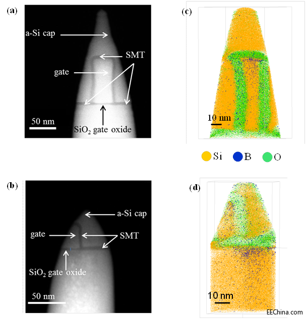
图1. DEVICE1的HAADF STEM图像(a) DEVICE2的HAADF STEM图像(b) APT和ET分析法要求将样品制备成针形。DEVICE1的APT体图 (c) DEVICE2的APT体图(d) 一个点代表一个原子。注:因为栅氧化层/衬底界面有针尖断裂,所以DEVICE1一直分析到栅氧化层。
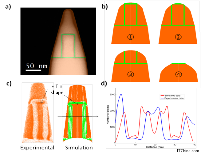
图2. a) 器件的仿真配置。STEM影像尺寸按比例放大。b)不同蒸发阶段的针尖形状变化 c) 作为实验和仿真对象的硅栅周围氧化区的重构图像。因SiO2相蒸发场高而引起的离焦效应导致氧化区厚度变大。注:SMT氧化区下面的栅区上部的T形状就是这些局部放大的结果。因为影像失真,所以没有提供放大影像。 d) 硅栅中心密度水平分布。低密度区与氧化区相关 (图2c中的绿色)。

图3: (a) 分割后的DEVICE1三维重构图像(b)原子探针层析法的氧重构体图(虚线)和电子断层扫描法的氧重构体图(实线)的合并图 (c)栅区硼分布三维APT图(蓝虚线) (d) DEVICE2栅极区、沟道和源/漏极区硼原子分布三维图(e) DEVICE2的密度修正式APT体图(f)沟道内1-D硼浓度分布图 (对应所选的原子分布插图) .
MOSFET 电子 仿真 集成电路 半导体 CMOS 电压 相关文章:
- 如何提升数字控制电源性能?MOSFET驱动器有办法(10-25)
- 基于单片机的脉冲快速充电系统设计(06-08)
- 硅光子带来新的设计挑战(07-07)
- 基于FinFET的SoC系统设计(02-11)
- 怎么能使Simulink的仿真速度更快?(08-19)
- IoT促进了低功耗的发展(12-05)