Help RF VC Oscillator Design
The Problem I seem to be having is that my sine wave is pretty for most of the cycle
but then abruptly jumps...
the output of the source followers is shown in the image below...
of course.. the input looks th same as well...
how do i fix this to get a full clean sine wave?
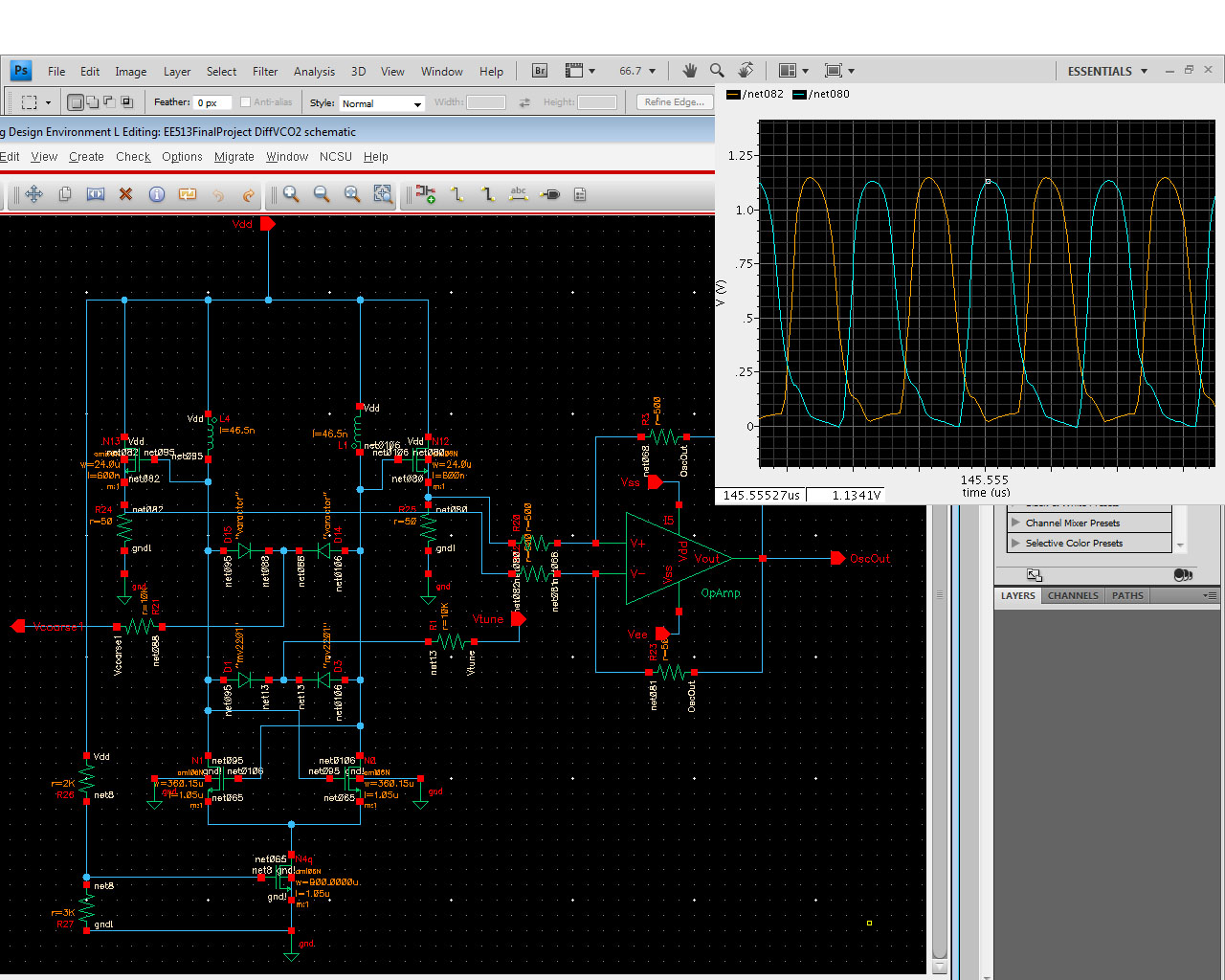
It's normal... you watch these wavefom single ended and differential oscillators create such waveforms.Because the voltage at each branch rises from zero and reaches to VCC but due to treshold voltages of the output source followers, waveform never drops to exactly zero.Around zero voltage, the MOS is almost OFF ( or weak inversion mode ) and just a leak is seen from the source side due to Cgs.
When you check out this waveform differential, you'll see pure sinusoidal shape.( If the OpAmp is well designed)
Thanks... I figured it has something to do with the op amp...
it doesn't work so well
it works as a simple noninverting or inverting config for simple amplication.. but when I try to use it as an active low pass filter it falls apart
i went through the design process I found in CMOS Analog Circuit Design by Phillip Allen and Douglas Holdberg...
section 6.3 design of a two stage op amp
the circuit consists of a PMOS current mirror feeding a two NMOS differential amp, with another NMOS tail for current, with the second stage of just two transistors, a PMOS and NMOS
I would post my design, but I am at home now and only have access to cadence at school.. will post later... but any suggestions would be greatly appreciated
any suggestions for improving the Op Amp?
Thanks so much
T.J.