virtuoso中Assura的LVS验证出现unbound的错误
时间:10-02
整理:3721RD
点击:
本人大三本科菜鸟,学习virtuoso版图设计中,用assura的LVS验证出现schematics与layout的unbound的错误,具体报错信息如下:

具体的log信息如下:
========================================================================
====File: diode_mimic.err
========================================================================
========================================================================
====File: diode_mimic.csm
========================================================================
Schematic| Layout| Status
-------------------------------------------------------------------------------
diode_mimic schematic practice| diode_mimic layout practice| errors*
Mismatch between Schematic and Layout
1 cell with errors
========================================================================
====File: diode_mimic.cls
========================================================================
*******************************************************************************
****** diode_mimic schematic practice<vs>diode_mimic layout practice
*******************************************************************************
Filter Statistics
=================OriginalFiltered
Cell/Deviceschematiclayoutschematiclayout
(ndio18, -) DIO1-*1-*
(-, ndio18) DIO-1*-1*
Reduce Statistics
=================FilteredReduced
Cell/Deviceschematiclayoutschematiclayout
(ndio18, -) DIO1-*1-*
(-, ndio18) DIO-1*-1*
Match Statistics
================TotalUnmatched
Cell/Deviceschematiclayoutschematiclayout
(ndio18, -) DIO1-*1-*
(-, ndio18) DIO-1*-1*
------------------------
Total1111
Match Statistics for Nets2200
==================================================================[diode_mimic]
====== Bad Matched Nets (don't really match) ==================================
===============================================================================
= = = = = = = = = = = = = = = = = = = = = = = = = = = = = = = = = =(badmatch 1)
Schematic Net:vdd!
S*1of ndio18 {PLUS MINUS}
Layout Net:avC1
L*1of ndio18 ?{PLUS MINUS}
= = = = = = = = = = = = = = = = = = = = = = = = = = = = = = = = = =(badmatch 2)
Schematic Net:gnd!
S*1of ndio18 {PLUS MINUS}
Layout Net:avC2
L*1of ndio18 ?{PLUS MINUS}
==================================================================[diode_mimic]
====== Problem Schematic Nets (no exact match in layout) ======================
===============================================================================
S
S ?vdd! ?gnd!
S (total 2) with:
S1of ndio18 {PLUS MINUS}
==================================================================[diode_mimic]
====== Problem Layout Nets (no exact match in schematic) ======================
===============================================================================
L
L ?avC1 ?avC2
L (total 2) with:
L1of ndio18 ?{PLUS MINUS}
==================================================================[diode_mimic]
====== Unmatched Schematic Instances ==========================================
===============================================================================
= = = = = = = = = = = = = = = = = = = = = = = = = = = = = = = = = = (schinst 1)
Schematic Instance: D0ndio18
S PinNet
S ------
S PLUSvdd!
S MINUSgnd!
==================================================================[diode_mimic]
====== Unmatched Layout Instances =============================================
===============================================================================
= = = = = = = = = = = = = = = = = = = = = = = = = = = = = = = = = = (layinst 1)
Layout Instance:avD33_1ndio18
L PinNet
L ------
L PLUSvdd!
L MINUSgnd!
==================================================================[diode_mimic]
====== Summary of Errors ======================================================
===============================================================================
SchematicLayoutError Type
-------------------------
22Bad Matched Nets
11Unmatched Instances
========================================================================
====File: diode_mimic.cps
========================================================================
; autoPinSwap() results for schematic network.
========================================================================
====File: diode_mimic.cfr
========================================================================
The LVS run "diode_mimic" has completed successfully.
Compare problems were detected in 1 cells.
1 cells had device mismatches.
1 cells had nets mismatches.
0 cells matched
No Extraction Problems were detected.
Press "OK" to enter the LVS Debug Environment.
Press "Cancel" to close this Dialog box.
LVS Run "diode_mimic"
is located in /home/guest/zzf
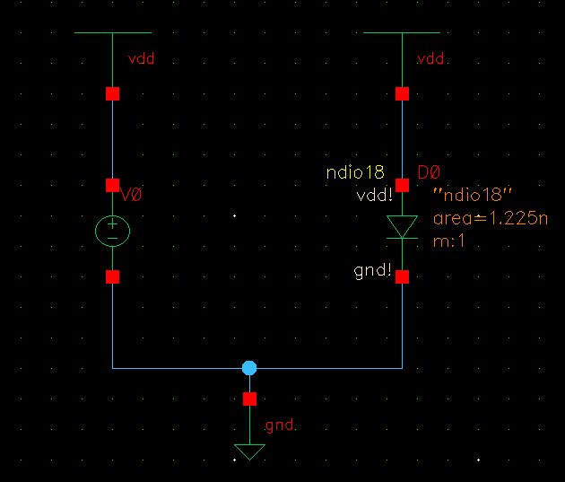
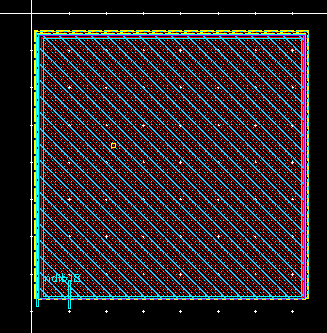
原理图和版图如下:
求哪位高人指点一下解决思路。
具体的log信息如下:
========================================================================
====File: diode_mimic.err
========================================================================
========================================================================
====File: diode_mimic.csm
========================================================================
Schematic| Layout| Status
-------------------------------------------------------------------------------
diode_mimic schematic practice| diode_mimic layout practice| errors*
Mismatch between Schematic and Layout
1 cell with errors
========================================================================
====File: diode_mimic.cls
========================================================================
*******************************************************************************
****** diode_mimic schematic practice<vs>diode_mimic layout practice
*******************************************************************************
Filter Statistics
=================OriginalFiltered
Cell/Deviceschematiclayoutschematiclayout
(ndio18, -) DIO1-*1-*
(-, ndio18) DIO-1*-1*
Reduce Statistics
=================FilteredReduced
Cell/Deviceschematiclayoutschematiclayout
(ndio18, -) DIO1-*1-*
(-, ndio18) DIO-1*-1*
Match Statistics
================TotalUnmatched
Cell/Deviceschematiclayoutschematiclayout
(ndio18, -) DIO1-*1-*
(-, ndio18) DIO-1*-1*
------------------------
Total1111
Match Statistics for Nets2200
==================================================================[diode_mimic]
====== Bad Matched Nets (don't really match) ==================================
===============================================================================
= = = = = = = = = = = = = = = = = = = = = = = = = = = = = = = = = =(badmatch 1)
Schematic Net:vdd!
S*1of ndio18 {PLUS MINUS}
Layout Net:avC1
L*1of ndio18 ?{PLUS MINUS}
= = = = = = = = = = = = = = = = = = = = = = = = = = = = = = = = = =(badmatch 2)
Schematic Net:gnd!
S*1of ndio18 {PLUS MINUS}
Layout Net:avC2
L*1of ndio18 ?{PLUS MINUS}
==================================================================[diode_mimic]
====== Problem Schematic Nets (no exact match in layout) ======================
===============================================================================
S
S ?vdd! ?gnd!
S (total 2) with:
S1of ndio18 {PLUS MINUS}
==================================================================[diode_mimic]
====== Problem Layout Nets (no exact match in schematic) ======================
===============================================================================
L
L ?avC1 ?avC2
L (total 2) with:
L1of ndio18 ?{PLUS MINUS}
==================================================================[diode_mimic]
====== Unmatched Schematic Instances ==========================================
===============================================================================
= = = = = = = = = = = = = = = = = = = = = = = = = = = = = = = = = = (schinst 1)
Schematic Instance: D0ndio18
S PinNet
S ------
S PLUSvdd!
S MINUSgnd!
==================================================================[diode_mimic]
====== Unmatched Layout Instances =============================================
===============================================================================
= = = = = = = = = = = = = = = = = = = = = = = = = = = = = = = = = = (layinst 1)
Layout Instance:avD33_1ndio18
L PinNet
L ------
L PLUSvdd!
L MINUSgnd!
==================================================================[diode_mimic]
====== Summary of Errors ======================================================
===============================================================================
SchematicLayoutError Type
-------------------------
22Bad Matched Nets
11Unmatched Instances
========================================================================
====File: diode_mimic.cps
========================================================================
; autoPinSwap() results for schematic network.
========================================================================
====File: diode_mimic.cfr
========================================================================
The LVS run "diode_mimic" has completed successfully.
Compare problems were detected in 1 cells.
1 cells had device mismatches.
1 cells had nets mismatches.
0 cells matched
No Extraction Problems were detected.
Press "OK" to enter the LVS Debug Environment.
Press "Cancel" to close this Dialog box.
LVS Run "diode_mimic"
is located in /home/guest/zzf
原理图和版图如下:
求哪位高人指点一下解决思路。
用的PDK是SMIC18MS的
已解决。修改Binding file.rul 即可。把schematic 和 layout中器件的名字改成自己实际定义的即可
请问你是去掉不要binding file 文件是吗?