这个ip核看着简单 oserdes 并转串 仿真失败
时间:10-02
整理:3721RD
点击:
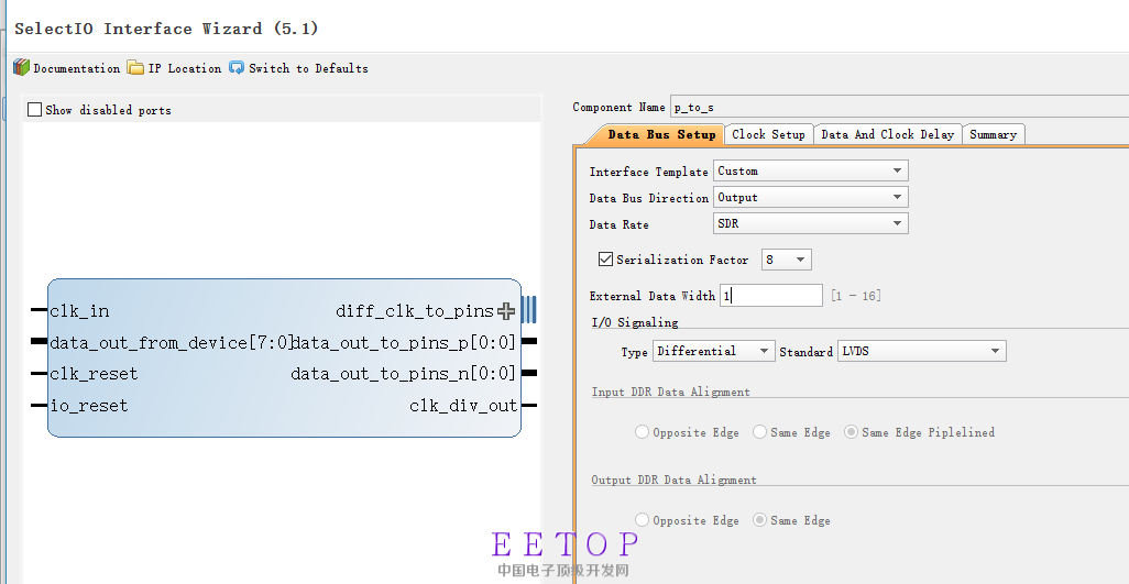
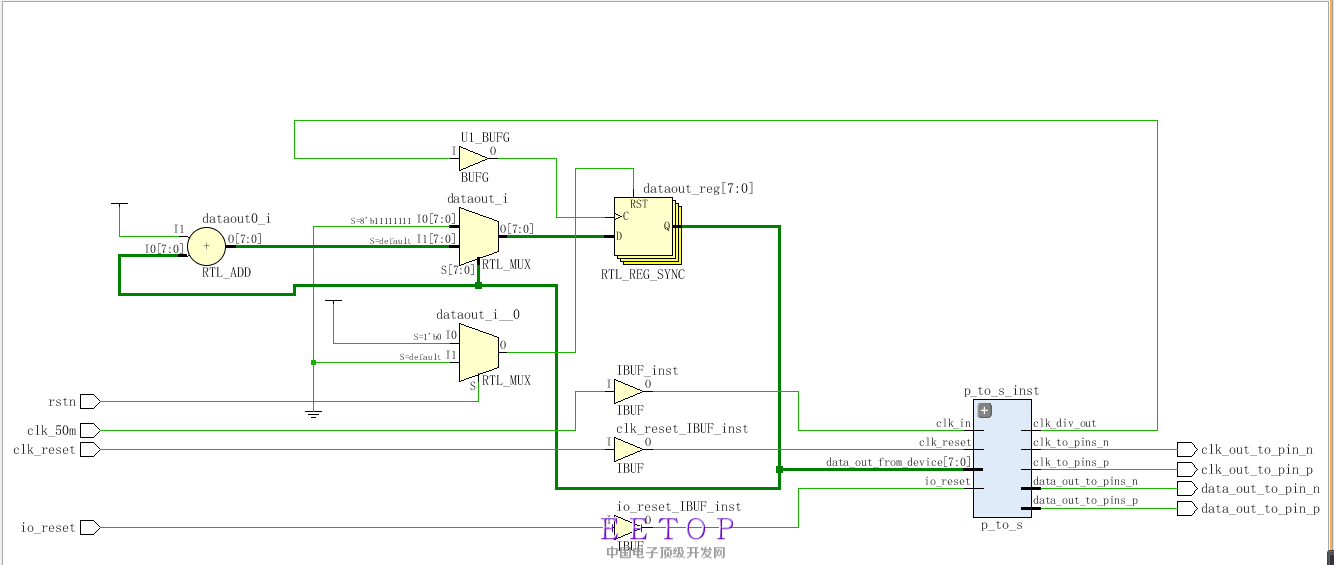
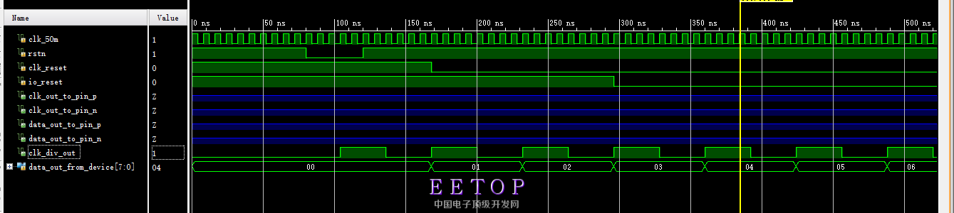
clk_div_out是有波形的,但是那些差分信号都没有波形。会不会是clk_in与clk_div_out之间的同步有问题。有做过的吗?给提供个思路吧,实在是没有办法了,看着挺简单的啊。不要只是看,给个回复,给个思路。
程序:简单的屁滚尿流
module Serdes_Test(
input clk_50m,//全局时钟
input rstn, //复位
input clk_reset,
input io_reset,
output clk_out_to_pin_p, //lvds时钟输出P
output clk_out_to_pin_n,
output data_out_to_pin_p, //lvds输出数据P
output data_out_to_pin_n //lvds输出数据N
);
wire clk_div_out_1; //低速时钟1,串行发送时钟的8分频
wire clk_div_out_2; //低速时钟2,串行接收时钟的8分频
//产生LVDS发送的测试数据,0~FF
reg [7:0] dataout=8'h0;
always @(posedge clk_div_out_2) begin
//always @(posedge clk_50m) begin
if (~rstn)
dataout <= 0;
else if (dataout == 8'hff)
dataout <= 0;
else
dataout <= dataout + 1'b1;
// dataout<=8'h9e;
end
//并转串,8位数据dataout转换成串行数据,并通过lvds差分信号输出
wire[7:0] dataout_w;
assign dataout_w=dataout;
p_to_s p_to_s_inst
(
// From the device out to the system
.data_out_from_device(dataout_w), //Input pins
.data_out_to_pins_p(data_out_to_pin_p), //Output pins
.data_out_to_pins_n(data_out_to_pin_n), //Output pins
.clk_to_pins_p(clk_out_to_pin_p), //Output pins
.clk_to_pins_n(clk_out_to_pin_n), //Output pins
.clk_in(clk_50m_1), // Single ended clock from IOB
.clk_div_out(clk_div_out_1), // Slow clock output
.clk_reset(clk_reset),
.io_reset(io_reset) //system reset
);
;
BUFG U1_BUFG(
.O(clk_div_out_2),
.I(clk_div_out_1)
);
//wire clk_50m_1;
IBUF IBUF_inst (
.O(clk_50m_1), // 1-bit output: Buffer output
.I(clk_50m) // 1-bit input: Buffer input
);
endmodule
激励:
module sim(
input clk_50m,//全局时钟
input rstn, //复位
input clk_reset,
input io_reset,
output clk_out_to_pin_p, //lvds时钟输出P
output clk_out_to_pin_n,
output data_out_to_pin_p, //lvds输出数据P
output data_out_to_pin_n //lvds输出数据N
);
Serdes_Test U1(
.clk_50m(clk_50m),
.rstn(rstn)
);
reg clk_reset_reg;
reg io_reset_reg;
reg rst_n_reg;
reg clk_50m_reg;
assign rstn=rst_n_reg;
assign clk_50m=clk_50m_reg;
assign clk_reset=clk_reset_reg;
assign io_reset=io_reset_reg;
initial
begin
rst_n_reg=1'b1; #80 rst_n_reg=1'b0; #40 rst_n_reg=1'b1;
// clk_50m_reg=1'b1; forever #4 clk_50m_reg=~clk_50m_reg;
end
initial
begin
clk_50m_reg=1'b1; forever #4 clk_50m_reg=~clk_50m_reg;
end
initial
begin
clk_reset_reg=1'b1; #168 clk_reset_reg=1'b0;
end
initial
begin
io_reset_reg=1'b1;#296 io_reset_reg=1'b0;
end
endmodule