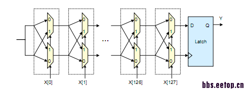
谁能给我解释一下这个电路图
时间:10-02
整理:3721RD
点击:

电路图的描述如下
Figure 1 illustrates a silicon PUF delay circuit based on
MUXes and an arbiter. The circuit has a multiple-bit input
X and computes a 1-bit output Y based on the relative delay
difference between two paths with the same layout length.
The input bits determine the delay paths by controlling the
MUXes. Here, a pair of MUXes controlled by the same input
bit X work as a switching box (dotted boxes in the figure).
The MUXes pass through the two delay signals from the left
side if the input control bit X is zero. Otherwise, the top
and bottom signals are switched. In this way, the circuit can
create a pair of delay paths for each input X.Toevaluate
the output for a particular input, a rising signal is given to
both paths at the same time, the signals race through the
two delay paths, and the arbiter (latch) at the end decides
which signal is faster. The output is one if the signal to the
latch data input (D) is faster, and zero otherwise.
大部分能理解,可是中间这个MUX如何工作的无法理解,MUX不是数据选择器吗,在这里如何使用啊。
功能是要生成随机数吗? mux就是为了把过程搞得更随机呗
观察下其实可以看到这些mux所有的数据端是一个,而选择端是X。X取不同的值时,后面latch的D端数据会经过不同级数的mux后到达latch,这就成为了1个物理延时路径。
看看,学习一下!
