例说FPGA连载39:DDR控制器集成与读写测试之FPGA片内RAM设置与集成
特权同学,版权所有
配套例程和更多资料下载链接:
http://pan.baidu.com/s/1c0nf6Qc
① Quartus II工程中,点击菜单“ToolsàMegaWizard Plug-In Manager”,创建IP核模块。
② 在弹出的选项卡中选择“Creat a new custom megafunction variation”,然后点击“Next”。
③ 选择我们所需要的IP核,如图4.3所示进行设置。
● 在“Select a megafunction from the list below”下面选择IP核为“Memory Compiler à RAM: 1-PORT”。
● 在“What device family will you be using”后面的下拉栏中选择我们所使用的器件系列为“Cyclone IV E”。
● 在“What type of output file do you want to create?”下面选择语言为“Verilog HDL”。
● 在“What name do you want for the output file?”下面输入工程所在的路径,并且在最后面加上一个名称,这个名称是我们现在正在例化的片内RAM IP核的名称,这里我们可以给他起名叫onchipram_for_ddr,然后点击Next进入下一个页面。

图4.3 单口RAM创建向导
④ 如图4.4所示,在第一个配置页面“Parameter Settings à Widths/Blk Type/Clks”中,我们需要做如下的设置。
● 在“How wide should the ’q’ output bus be?”后面输入“64”bits,即该片内RAM的存储位宽是64。
● 在“How many 64-bit words of memory?”后面输入“256”words,即该片内RAM的存储深度为256。
● 在“What should the memory block type be?”下面可以选择“Auto”,也可以选择“M9K”,表示我们的RAM是使用FPGA固有的片内存储器资源还是逻辑(LCs)资源。
● 在“What clocking method would you like to use?”下面选择“Signal clock”,表示该RAM的读操作或写操作使用同一个时钟。
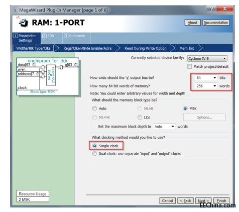
图4.4 RAM参数设置1
⑤ 如图4.5所示,在第二个配置页面“Parameter Settings à Regs/Clken/Byte Enable/Aclrs”中,做如下设置。
● 在“Which ports should be registered?”下面选择“’q’ output port”,表示‘q’信号输出时会用时钟clock打一拍,这样更有利于时序收敛。

图4.5 RAM参数设置2
⑥ 第三个配置页面“Parameter Settings à Read During Write Option”可以不用理会,默认设置就好。
⑦ 第四个配置页面“Parameter Settings à Mem Init”则需要特别设置一下,如图4.6所示。
● 在“Do you want to specify the initial content of the memory?”下面勾选“No,leave it blank”。表示我们不需要设置RAM的初始化文件,当然了,在某些特殊应用中,设计者希望有初始化RAM文件,那么可以勾上“Yes,use this file for the memory content data”选项,然后在高亮的“File name”后面选择初始化RAM文件。
● 勾选上“Allow In-System Memory Content Editor to capture and update content independently of the system clock”,因为我们在板级调试时,将会用到In-System Memory Content Editor工具来实时查看RAM中的内容变化。“The ‘Instance ID’ of this RAM is:”后面随便输入一个数据,如我们输入“7788”,这个数据类似一个ID号,它主要是区分In-System Memory Content Editor工具查看不同的RAM。
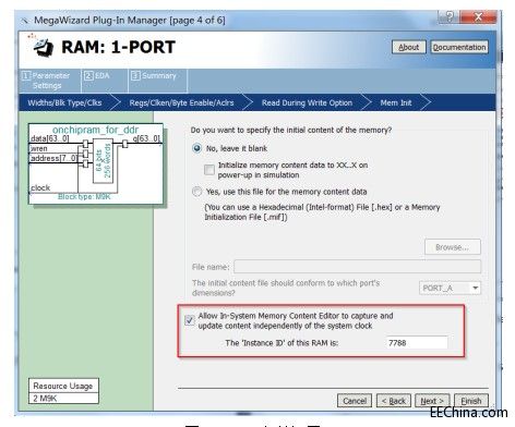
图4.6 RAM参数设置3
⑧ 最后,在“Summary”页面中,如图4.7所示,勾选上“onchipram_for_ddr_inst.v”文件所在选项。点击“Finish”完成设置。
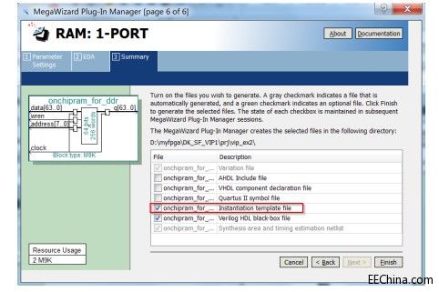
图4.7 RAM配置Summary页面
onchipram_for_ddr_inst.v文件打开如图4.8所示,这里有新建RAM的接口例化模板,可以复制到工程顶层源码中重新做接口映射。

图4.8 RAM IP核例化模板
- 基于FPGA的片上系统的无线保密通信终端(02-16)
- 基于Virtex-5 FPGA设计Gbps无线通信基站(05-12)
- 基于FPGA的DVI/HDMI接口实现(05-13)
- 基于ARM的嵌入式系统中从串配置FPGA的实现(06-09)
- 采用EEPROM对大容量FPGA芯片数据实现串行加载(03-18)
- 赛灵思:可编程逻辑不仅已是大势所趋,而且势不可挡(07-24)