negative resistance
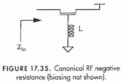
image from the design of cmos rf integrated circuits-2nd ed (Cambridge, Lee, 2004) page 642
inductance in the gate circuit of a common-gate device can cause a negative resistance to appear at the source terminal
how you prove that? (how you show that?)
Theorotical:
Convert S parameter in to Z parameters.
Add XL that is inductance to Z parameters
Again convert to S parameters.
If your S11 is >1 means you have obtained negative resistance.
You find the details about the explanations in following books
You can tally this using S11 equation. (zin-zo/zin+zo)
1) Microwave transistor amplifiers by gonzalez
2) microwave devices & circuits by Lio PHI publication
If you want to see this practically
Use simulators such as ADS
there you can directly check using tools
Here is an attempt for an obvious and evident explanation of the effect:
A negative resistance can be thought of a voltage controlled current source which drives a current back into the voltage source.
In the circuit shown this can happen when a voltage at the source pin drives a current into the FET which causes a small current through the GS capacitance and the inductance between gate and ground (for rather high frequencies).
As a result, a voltage is created across the inductance which in turn causes a drain current (normal FET operation) which goes into the voltage source at the source pin. Thus, for a certain frequency range this circuit has a negative input resistance at the source pin.
Or you can consider this structure as a three port device. When you calculate 3 port s-parameters by adding a reflection coefficient at third port ( see Solid State Radio Design-I.Bahl, Prakesh et al.) you'll see S11>1 that is equivalent to negative impedance..
resistance 相关文章:
- Adding ports to know resistance at some point in 2-patch antenna
- Microstrip Negative Resistance Oscillator Nyquist plot Encirclement issues
- What is the gate resistance of the LDMOS?
- Calculating Resistance/Capacitance values from measured/simulated S-parameters
- MOSFET Resistance rout and Rds (ON)
- Negative resistance oscillators that designed wrong