momentum optimization
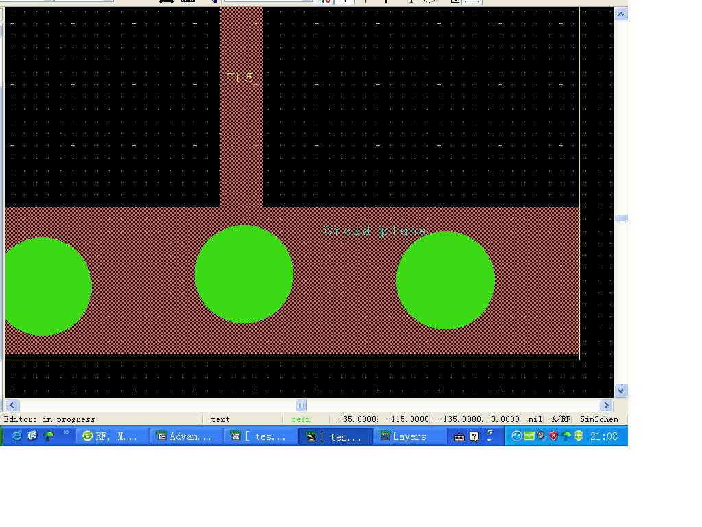
I am newbie.I want to optimize the length of TL5,I have a question:when TL5's length increase,whether the ground plane will auto change correspondingly.if not,how can i set the ground plane?
Thanks,
It is not clealy visible,
what the other end circuit?
Share the design
Thanks firstly.I want to optimize filter in Momentun.I want to set TL5 length as parameter.i TL5's length increase,whether the ground plane will auto change correspondingly?so that the increasing length of TL5 is effective.
Thanks,
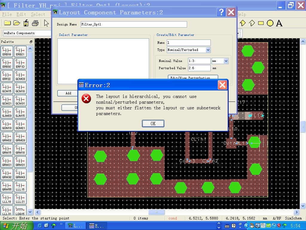
This problem is first simulated with schematic components then edited in Layout for
GND or any other requirement. Is my understanding is correct?
But I observe that he components are not flattened.
This is necessary to de-link the schematic component.
Then you do the parametrization in layout
Thanks kspalla.you are right,it is simulate with schematic.and how to de-link the schematics.I had a trial that copy the layout file and re-create a new project to optimize,but still fail.Attached my file .
Another hand,the schematic simulation result is more different with co-simulation,so confused.which one is believable?
Anyone has experiments about microstrip optimization in momentum?
I opened the file and noticed that you are primitive to layout work.
I suggest you to carry the simple structures in layout for better understanding.
There are lot of examples under momentum section in ADS.
Thank kspalla for your suggection.
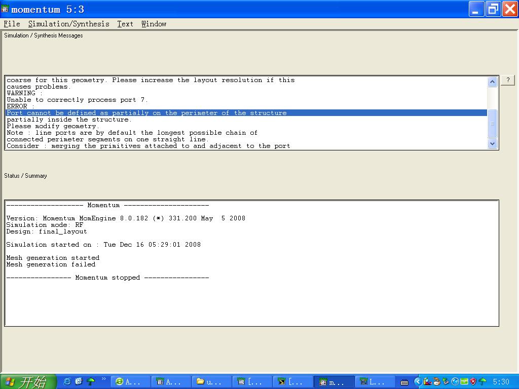
En...the upload file is unpratical,only for studying momentum optimization.The structure is similar to our design schematics that include lump components and microstrip mixed circuit and the example project in ADS is lack of this type example .I met more different cases and confused cases.For example,if the parallel microstrip that connected to ground) is optimized(the length increase),how to deal with the ground planar and vias(are they also synchronized automatically or i need to set the ground optmization) ;place the ports to C16(port 7),and run simulation,it indicated error ports(as attached) ,and i do not know how to fix them.
I appreciate all of you can help me.
Hi,
I gone through the circuit.
The circuit is taking much time to simulate so I have not simulated it but giving you the component.
I modified the layout based on
1)component placement
2) Vias should be closer to line
Let me know
1) Any problem you face in simulating the structure
2)Whichh part you want to tweak
a) lower side
b) upper side
c) both lower and upper part of circuitry.
Thank kspalla's warmheated help,your documents give me more clear about optimization.I want to tweak lower side.There are three types:short stub(TL4 wiht ground),the length of CLIN1,and microstrip(TL11) in series with capacity.My confusion is the perturbation area selection.Does it include ground plane and via?And whether the via need to be flatten firstly?
Another question,when i select an object in the layout to apply the perturbation ,whether it include the port that i placed it in the pad?
You need to select Via which is near GND and partly GND plane depend on the direction.
No need to do further flatten as I already did for you.
Yes if the port is connected to the object.
I fixed it now.Thanks for your help sempre.