Area Pin in momentum Simulation - ADS
i want to simulate a PCB with area pins in ADS and found that article:
http://muehlhaus.com/support/ads-app...edge-area-pins
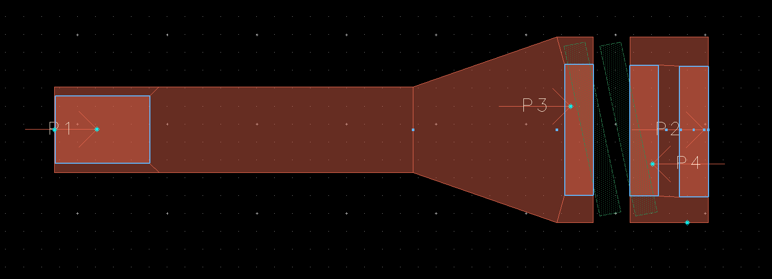
I did exactly the same.. Unfortunately I got some warnings at momentum simulation. Here is my Layout with area pins at the input and output of the stripline and two area pins before and after a gap. This is necessary to simulate a inductor or capacitor (just SMD elements).
And here is the warning message:
Anybody knows what these two error messages mean? Are they important or can i ignore them? The last one occurs for every port. The areas of the ports are exactly at the edges of the stripline.. Im not really sure if my pin connection is correct. The first setup was with TML calibration at every port.
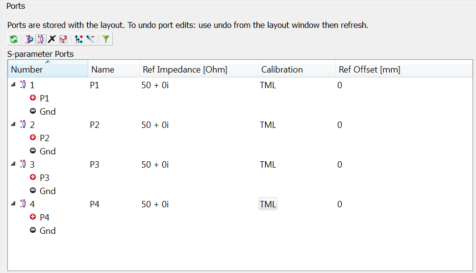
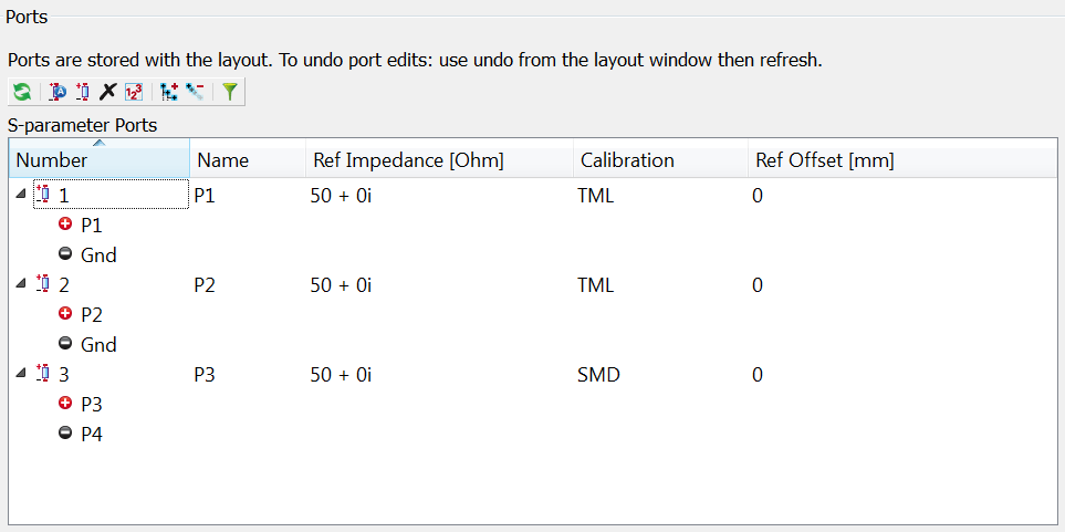
The second setup was with TML for port one and two, port three and four was configured with SMD calibration.
Is the last setup the right one, if i only want to simulate a SMD inductor or capacitor (with s2p files)?
Best regards
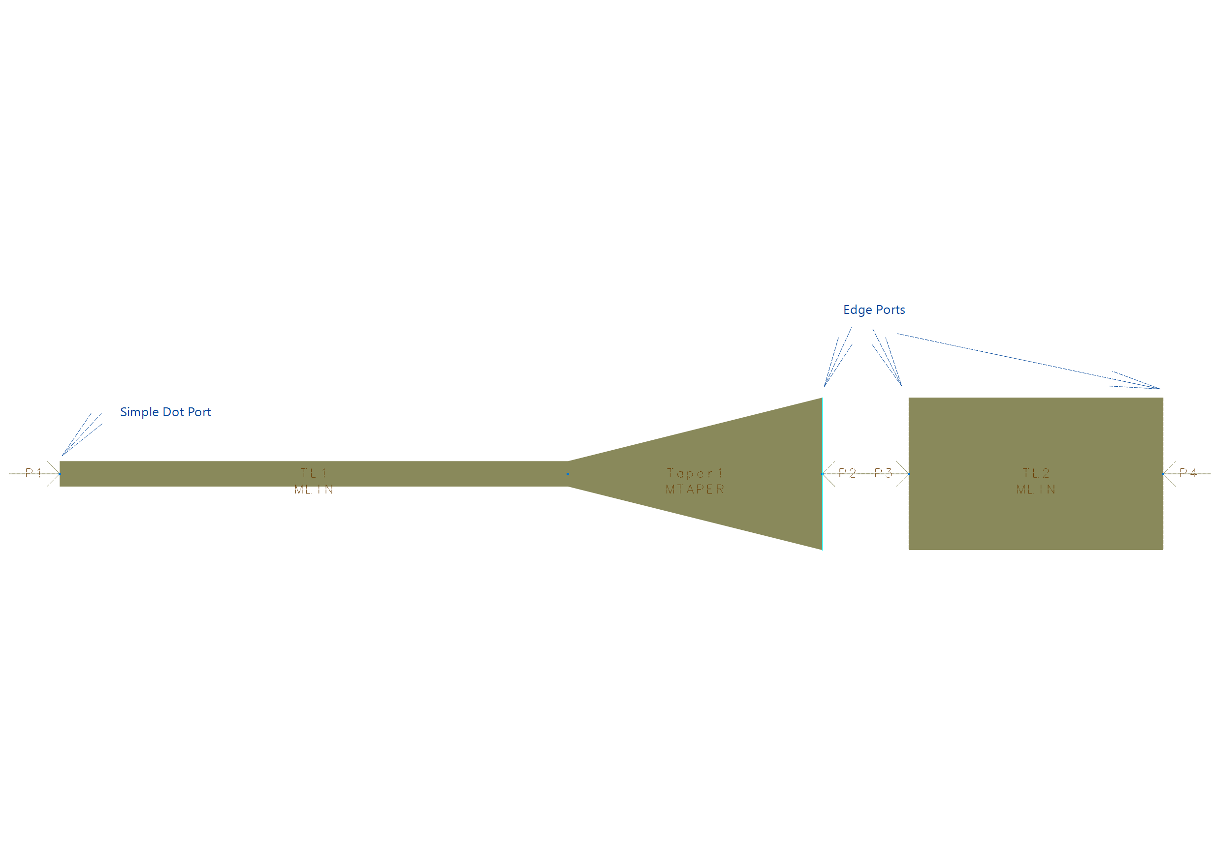
Area Ports should be placed at the edge of the layout,not at an internal point.
The reason of using this area port is to spread the port calibration are through layout edge.
Thank you for your answer! I found out, that there is an example of the different calibrations if you hold the mouse for some seconds at the calibration dropdown menu. There are some pictures for the corresponding setup.
But what is the right way to simulate? In the my layout (nearly the same as in the picture above), I got a 1.2mm x 5mm stripline prepared for a SMA connector (1mm x 5mm). I thought that I have to set up an area, because my pin is not at the edge of the stripline. The same applies for the inductors and conductors that I want to measure.
Second question was the pin configuration for the SMD element.. What is the right setup (picture 2 or picture 3) ?
You complicate the problem.All you should do is to place right port config.
okay thank you. is it important to choose the right order of the pins? you got pin2 at the end of the taper.. i found many examples with pin1 and pin2 at the beginning and end of the stripline, with the other pins in between.
No matter what orders they are.The ports are principally placed beginning from 1 at most left ( input ) to n at most right ( output ) for a better organization.
It doesn't matter if your SMA center pin overlaps with the line, that behaves line one conductor in the overlap region. Your port is where the signal from the SMA first contacts the line.
The edge/area port in the application note (post #1) is most relevant if the metal edge is much wider than the connected component pin. Example as shown in the appnote: power transistor lead connected to wide stub. Then, we really need to control the port width. For the case shown here in this thread, there is not much effect.
This is approximately correct. To be precise, it depends where the reference plane of the SMD devices is. Unfortunately, for S2P data from component libraries we often don't know the component reference planes.