RF tranmitter's problem
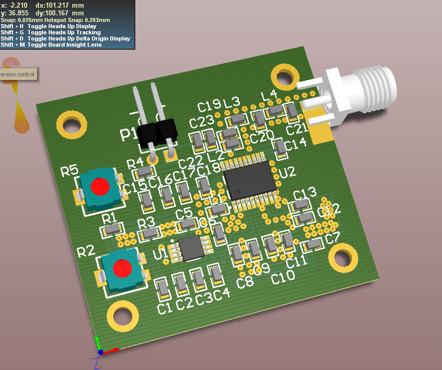
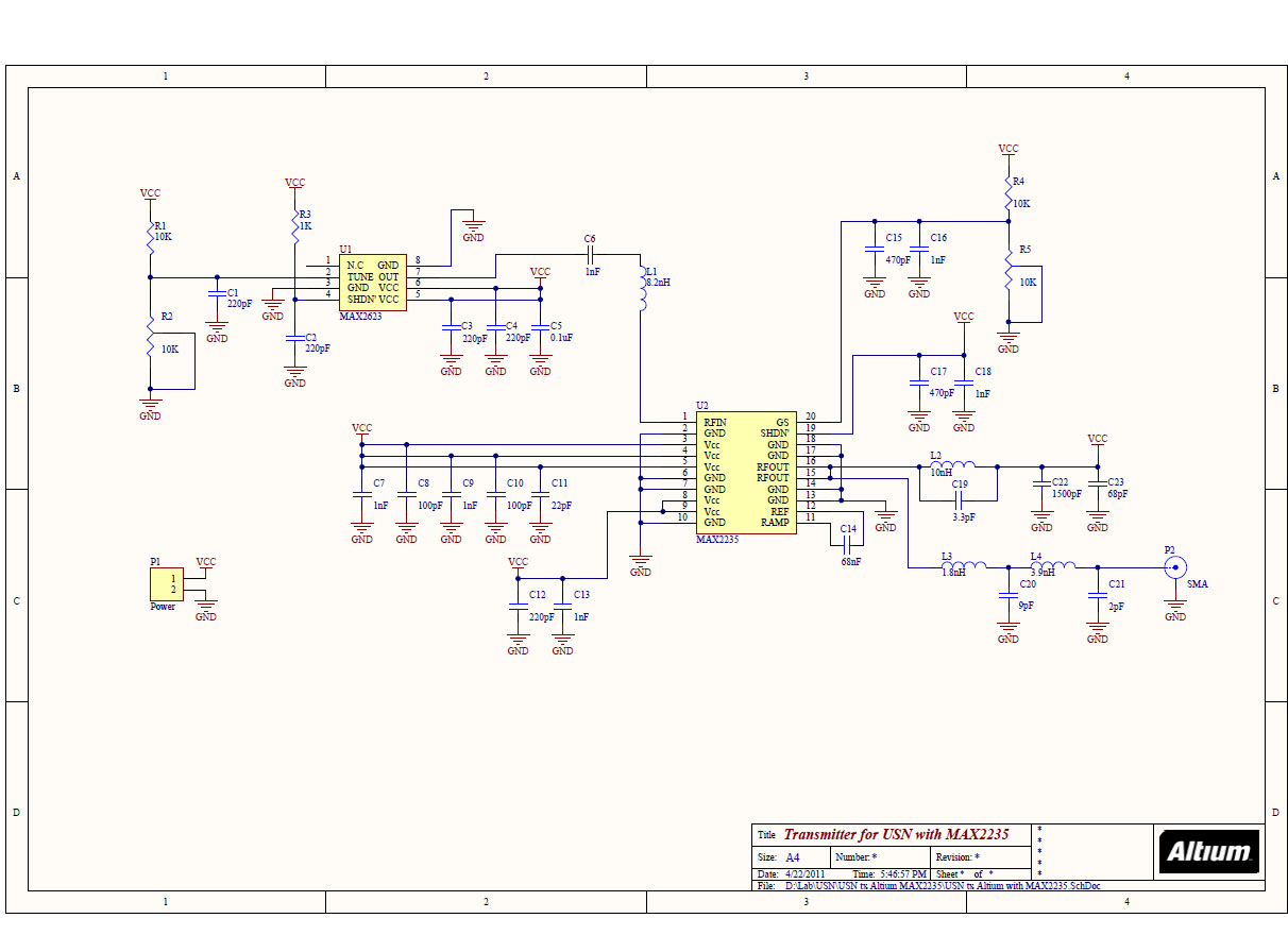
I'm making a RF transmitter, which transmits just power no data. It operates at 915MHz. The transmitter consists of a VCO (MAX2623), a power amplifier (MAX2235).
My goal is 1W (30dBm) output power. But my transmitter's output power cannot be 1W. It's just 20mW (13dBm). I used the coplanar waveguide with ground (50 ohm). Also i connected exposed paddle of the power amplifier to ground via hole.
The biggest problem is heating. The power amplifier becomes very hot.
I don't know why it is not working well
Please help me
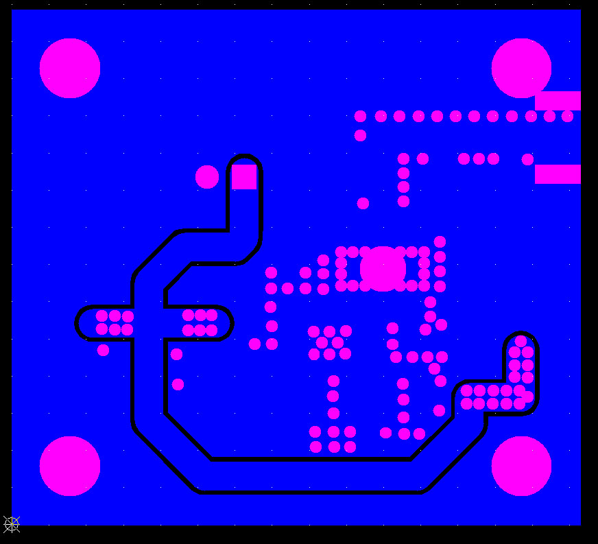
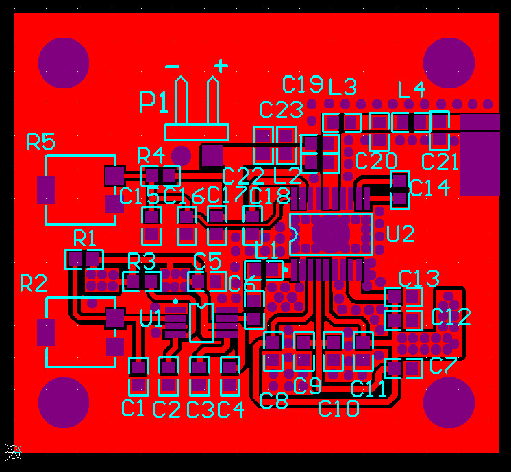
These are my PCB layout
[IMG]
Fisrt of all, I would like to see the exact circuit.
Hi
thanks for reply
[IMG]
Coplanar waveguide (50ohm transmission line) is used in this circuit.
I think you forgot the output series capacitor (from pin 15 of U2 to L3) to avoid the DC flowing through the load.
And you should add heatsink for the PA.
Hi guys
Thanks for reply and suggest
I used the via hole under the PA and i soldered it to exposed paddle. The via hole can be heat sink according to datasheet.
---------- Post added at 10:23 ---------- Previous post was at 10:19 ----------
Hi guys
Thanks for reply and suggest
Yes your right i forgot the capacitor (DC block). I have connected the capacitor between the SMA and C21. It has no difference.
I think the issue is in interstage matching of the 3 PA stages. The traces lenght between VCC pins and decoupling capacitors are fundamental for this matching.
Read very carefully this: MAX2235—Layout Optimization Techniques - Maxim, I'm referring in particular to fig.1 and fig.2. Use the same layout and cap series they suggest.
I hope it can help.
Mazz
No ... put it between pin 15 and L3 ... it would be preferable to keep the DC away from the filter stage. no point having it going anywhere where it isnt wanted/needed
it is possible that because you didnt put the cap in, before testing, that you have already damaged the MAX 2235
Dave
@Dave
did you mean a non-electrolit capacitor?
yes, say a 1nF ceramic/etc SMD type like being used for C7, 9, 13 etc
additionally, I see they have the DC blocking cap on the output of the filter. I still in my work prefer to keep DC out of places its not needed
Dave
Hi Mazz
Thanks for reply
I have already read the Lay out optimization techniques and tried to follow the suggestion.
I used 2 layers PCB. It was difficult to follow all of suggestion especially (fig.1 and fig.2) due to 2 layers.
What should i do?
---------- Post added at 14:01 ---------- Previous post was at 13:52 ----------
Hi guys
Thanks for reply
I tried an output circuit of MAX2235—Layout Optimization Techniques. But no difference.
What should i do?
Is there anybody? who have experience of RF circuit and MAX2235
---------- Post added at 14:03 ---------- Previous post was at 14:01 ----------
hi Dave
Thanks for reply
What should i do? Do you have any idea?
I've seen that you have applied most of the suggestions given in the app.note, and the solution you've found with the two layer is not so bad.
You should keep VCC tracks very short, just as shown in fig.2.
Are you sure about VCO output power? I've seen in the VCO layout some possible issues. My suggestion is to follow layout example given in the MAX2622 eval board.
Keep VCO output far from PA supply tracks.
I hope it can help.
Mazz
Are you sure you ICs are still working (mainly max2235) ? Did you try to replace them ?
Are you sure there are no errors in you PCB, with respect to the schematic diagram ?
Hi guys
I have replaced the PA(MAX2235). I measured output power of VCO. The output power was -7dBm when i measure it.
I don't know why output power cannot be -3dBm. Maybe VCO was damaged. I didn't replace it.
But another VCO (MAX2623) is working well that is placed another PCB board (Pout=-3dBm).
So i amplified it up to 14dBm by WJA1500 that is called gain block.
The maximum input power of PA(MAX2235) is 13dBm. So i had have to reduce the output power (Pout<13dBm).
I put 100 ohms resistor on output's coplanar waveguide (transmission line) to reduce the power.
The output power of WJA1500 was reduced up to 7-8 dBm.
In the end i connected MAX2235.
So i have obtained 30dBm (1W) RF power. But efficiency is very bed. It is just 25%.
---------- Post added at 17:02 ---------- Previous post was at 16:57 ----------
Hi albbg
Thanks for reply
Some ideas about low efficiency.
Maxim is not specifying the optimum load for class E operation, as they declare in the datasheet, but they only give some indication in the application circuit.
It seems that the load they use in their board is roughly 5-j20 at 850MHz. So we can assume that the 47% efficiency is obtained using this load. Be careful that they use very high quality capacitors from ATC for DC blocking and matching.
I haven't analized the LC network you are using, but, at a first glance, it doesn't take care about this optimum load for the PA.
This can be the reason for the lower efficiency.
I hope it can help.
Mazz