Impedance matching on my 802.15.4 board
时间:04-07
整理:3721RD
点击:
Hi,
I am trying to design the RF part of an 802.15.4 board with ATmega128RFA1. This is my first RF design and I need help from someone more experienced.
First, I want to know the dimensions of the 100ohm differential trace to the balun. I use Sonnet simulator but I am not sure if i use it the right way. I will describe what I do step-by-step. Please let me know if I miss something.
1. I have chosen the dielectric layers: 1000mils of air above the board and FR4 (30 mils of board). Below the trace is the ground plane.
2 .I moved the sides of the box away from the traces.
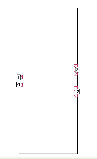
3. I have drawn the footprints of the IC and a balun, and added two 100Ohm ports: 1,-1 and 2,-2
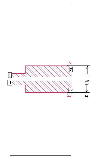
4. Next, I have drawn the differential line. I left the 10 mils gap (the same as the IC pin spacing), while the width is parametrized.
5. Finally, I set up the the parameter sweep analysis ( 10 to 50 mils, 5mils step @2.45GHz). I get the following results
According to that I will choose 30 mils width for my board.
Before I proceed to the next step (balun to antenna), I want to know if my procedure described above is OK.
Then I'll have some more questions
I am trying to design the RF part of an 802.15.4 board with ATmega128RFA1. This is my first RF design and I need help from someone more experienced.
First, I want to know the dimensions of the 100ohm differential trace to the balun. I use Sonnet simulator but I am not sure if i use it the right way. I will describe what I do step-by-step. Please let me know if I miss something.
1. I have chosen the dielectric layers: 1000mils of air above the board and FR4 (30 mils of board). Below the trace is the ground plane.
2 .I moved the sides of the box away from the traces.
3. I have drawn the footprints of the IC and a balun, and added two 100Ohm ports: 1,-1 and 2,-2
4. Next, I have drawn the differential line. I left the 10 mils gap (the same as the IC pin spacing), while the width is parametrized.
5. Finally, I set up the the parameter sweep analysis ( 10 to 50 mils, 5mils step @2.45GHz). I get the following results
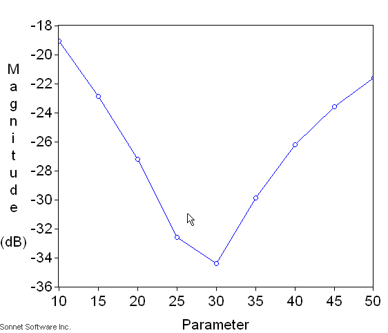
According to that I will choose 30 mils width for my board.
Before I proceed to the next step (balun to antenna), I want to know if my procedure described above is OK.
Then I'll have some more questions
You did the right thing, and for 100 ohms differential impedance, 30 mils trace width should be fine in this situation.
EM simulators are the best for simulating differential traces, but there are available few simple/freeware programs which are doing the same thing.