input matching before/after load pull simulation
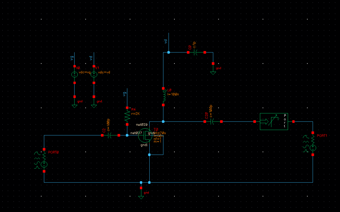
I have a question regarding load pull simulation. After obtaining the Zload for optimum power (at this point my input is not matched yet) i did the matching for output, i went on to conjugate match my input but the results were terrible with the S21 going below -5dB (supposed to be about 10dB). That happens if i did my input matching after load pull. Should i conjugate match it first before load pull simulation then? Advise please. thanks in advance!
natnoraa
You should find a compromise between 2 matching circuit.Either you optimize your PA with less Power Output and higher Gain compare to Maximum Output Power and Efficiency or you shift your matching circuit to obtain higher power but lower gain or between these two..
But even you obtain a matching circuit which gives you max. power S21 shouldn't be very bad.Check out your configuration.There should be an error..
I have never encount the problem like you. I think there should be some problem with your inut matching circuit.
You followed the right scheme!
better check your input matching!
thanks for the inputs bigboss and justtry114. Am working on a class a amplifier and it looks like a bilateral case. will try the higher gain but lower power matching configuration and look at the results again. am using cadence virtuoso for the design so it's a lil' not as 'user-friendly' for rf design as compared to ads.
thanks for giving me a lil' confidence smoothcriminal! the irony is that my input shows that it's well matched?
I have included some screenshots for your perusal:
1) original circuit
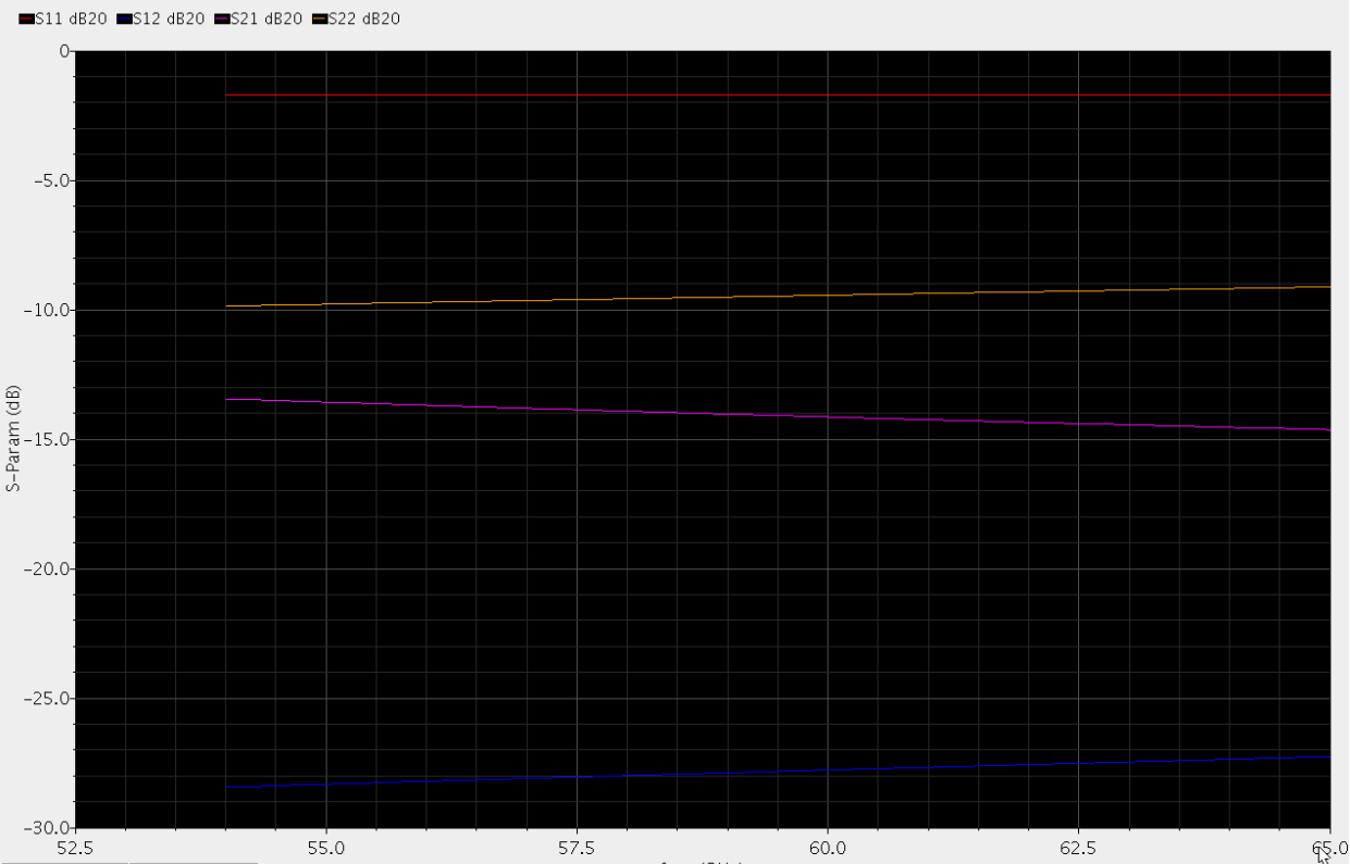
2) initial s param
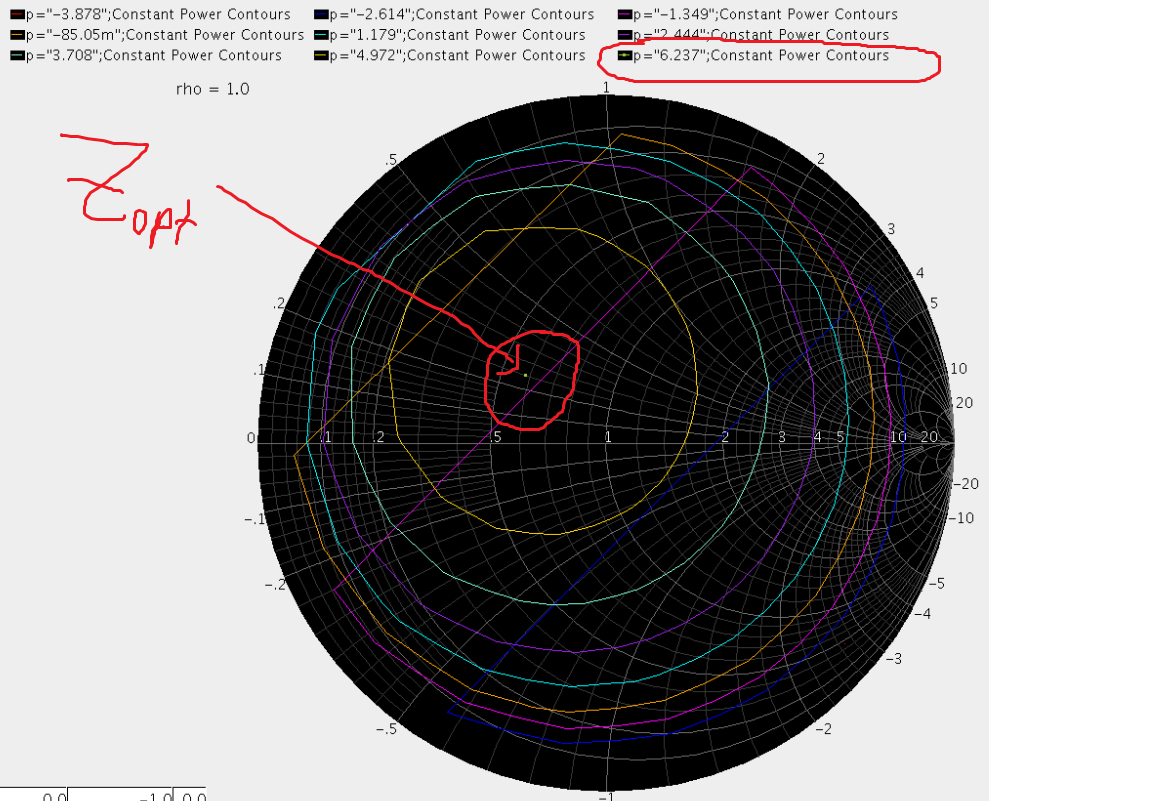
3) load pull simulation showing Zopt
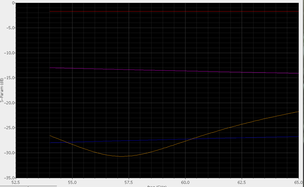
4) s param after output matching
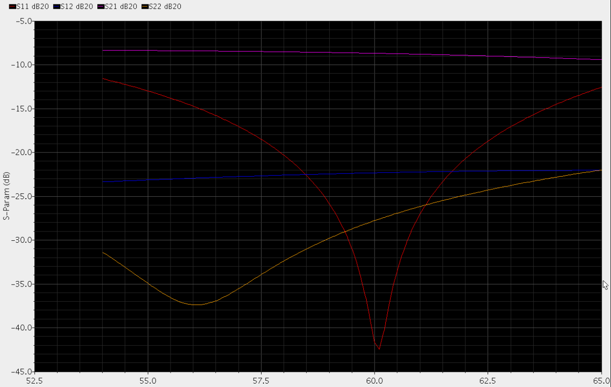
5) s param after input conjugate matching from checking ZM (real and imaginary)
6) operating point of transistor (made sure it's in saturation)

the results show good S11 (input matched),S12 and S22 (output is okay) but very very poor S21 (in fact to begin with it's already bad).
there's no sensitive information so am sharing the steps and hopefully someone can see what's wrong with them and give me some guidance. thanks!
P.S : one more question, if the matching network is supposed to have a capacitor (in the place of my dc block cap), can i just replace it with the value i wanted? (the initial dc block cap has value way higher than the current value i want for eg.)
natnoraa
going multi-fingers design actually solved the s21 problem... which am still clueless why. more fingers means higher parasitic cap and which will result in poorer performance but why does it enhance S21?
