How to design differential LNA input match?
I want to design differential input match network.Datasheet give me the input port impedence as attached.and I do not know how to match with differential case. My question is in the attached pictures.I need your kindness help me.
And i am lack of differential impedance match,anyone can share me some documents introduced differential port match?
Many thanks in advance,
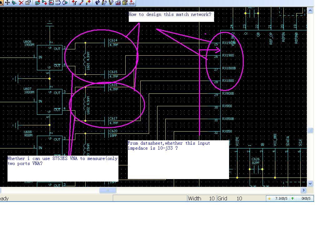
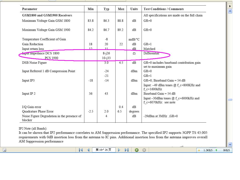
If i make the match network?which impedance i should match,10+j*33 of 10-j*33 to get good NF?
Thoughs are differential output SAW filters in front of IC. The matching is to get from the SAW output Z to IC input Z. It should be conjugate match so it is resonate at operating frequency.
SAW's need to be terminated with proper Z to get proper response so you ahave to go with conjugate match.
Keep in mind that at 2 GHz PCB layout strays will significantly effect the match.
Differential matching is no different then single ended matching. Just split series cap or inductor in two on either side with half the calculated value.
Welcome - Microwave design articles, applications, and high-frequency design techniques for microwave and wireless engineer
http://www.wless.ru/files/433-868Mhz...427%20v0.1.pdf
Thank RCinFLA and vfone for kindness.
Hi every body
You can help me ! I use http://www.wless.ru/files/433-868Mhz...427%20v0.1.pdf but not true because form SWA to LNA is differential.
differential design LNA 相关文章:
- Loadpull for Differential PA
- How come differential cascode structures affect on PA characteristics?
- Microstrip differential impedance depending on line width
- Differential Input For Dickson Chgarge pump Rectifier
- Multiband Differential Rectifying Circuit (re symmetry or not)
- Differentially-Fed Rectifier