SMA connector, on which side of a pcb?
I'm designing a two-layer pcb with an RF module on it (
The first one: although the impedance of the microstrip line will be 50 ohm for most of its length, it won't be 50 ohm when entering the sma connector. This problem is exactly the same (except for smaller sma and lower frequency) as the one I found on this blog: http://www.rowetel.com/blog/?p=147.
The second one: Since the sma connector is placed on the top layer the antenna doesn't directly "see" the bottom layer RF ground plane. The ground plane is obstructed by top layer components and traces.
Well, I'd like to know if I can place my sma connector this way. I mean, will the rf performance be seriously compromised by doing so? Or should I definetely avoid this kind of configuration and place the sma on the botom layer side?
Thank you very much for any practical advice because I'm completely at a loss
Why don't you use edge mounted SMA connector ?
Like this http://store.ckdevices.com/products/CMP-324.html
Well, I could but it would complicate my project a lot because of some enclosure size and mounting constraints. I'd like to use straight sma if disadvantages of that kind of placement aren't significant.
if it has to be a connector at right angles to the board where u drew it, then you have the right idea.
you can use a thru hole type SMA, and still run the traces on the top (RF) side of the board. just make sure the body of the connector does not short out the line (need an air gap), the soldering of the thru pins can be done on the backside (if u have plated thru holes), and insure that the ground plane pour is at least 30 mils away from the 5 thru holes center contacts!
Alternatively, you can use a surface mount style SMA. It has 5 soldering pads, instead of 4 thru hole pins. This type already has a bump in the metal body to not short out the 50 ohm trace as you solder the connector over it.
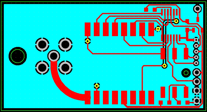
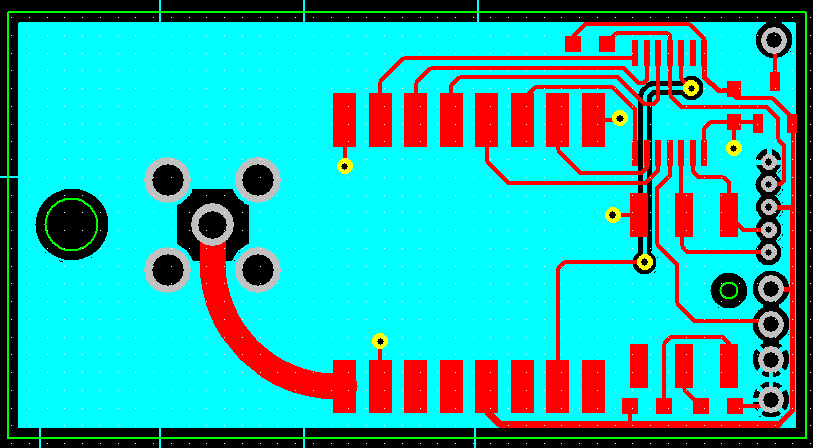
Thank you biff44. I didn't really notice this spacing problem. Now I made the center contact 33 mils away from the ground plane pour (

An error of reasoning. The antenna will "feel" the ground plane anyway, wether it's on top, bottom or inside the PCB.
The impedance mismatch of the connector transition will be small and negligible related to the mismatch of the antenna input in combination with the insufficient groundplane size.
In additional to these comments..
Put vias as much as possible everywhere to improve the GND connection of TOP layer.And don't use thermal relief for SMA connector,instead tie the GND connection with poured thruhole pads.
I corrected the pcb design (
Preferably supply copper pours should be bypassed to ground plane by a number of capacitors.
- Question about PC3.5mm and SMA connectors
- SMA to SMA connector
- How to use field replaceable SMA connector for best data.
- lines width versus the width of the component's connectors
- Is there any SMA Connector Model available ?
- HOW to chose coaxial cable and connector for prob feed patch antenna at 5.8ghz