finite ground plane with global or differential ports
Here are my layout and substrate setup and schematic with finite ground plane.
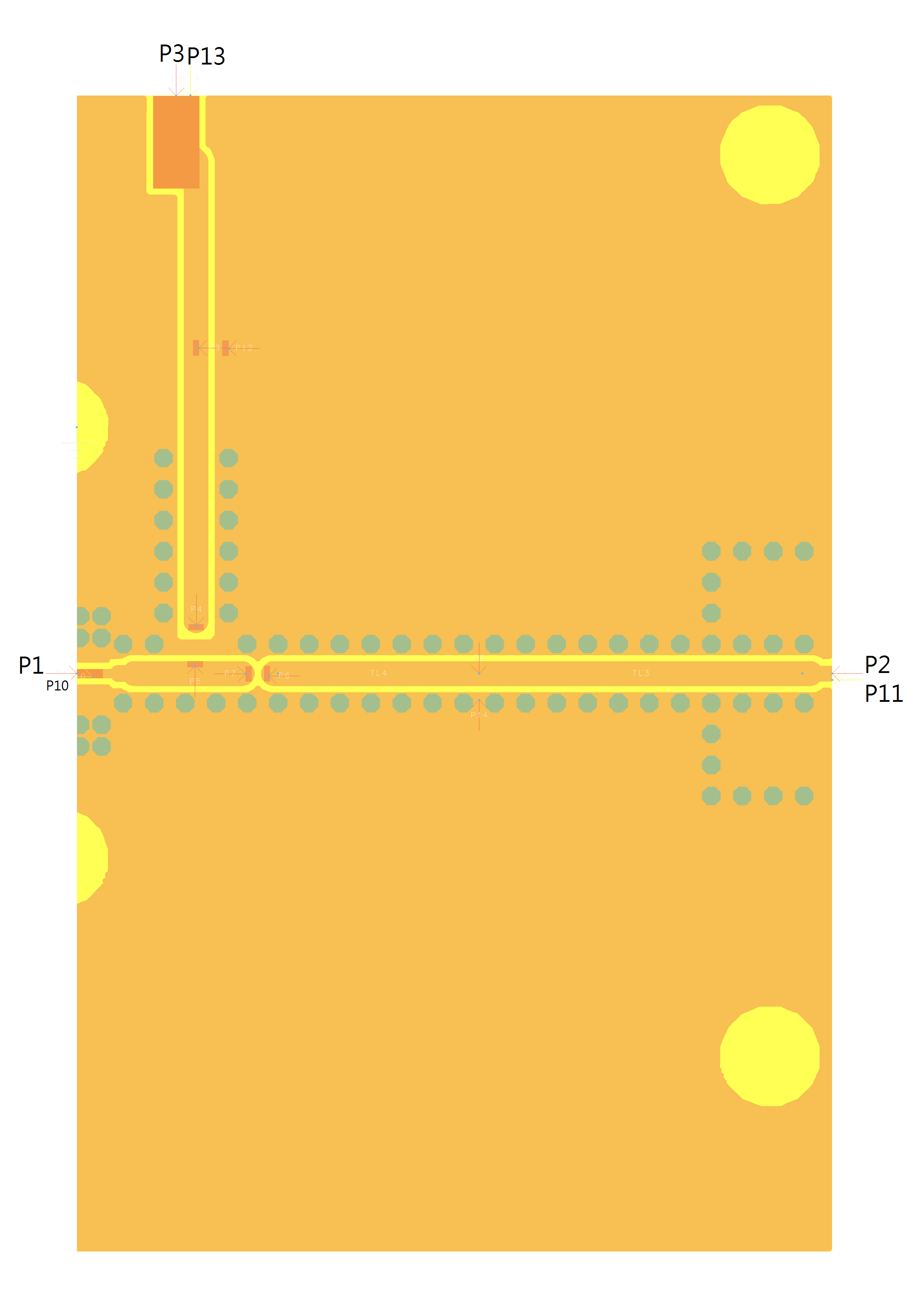

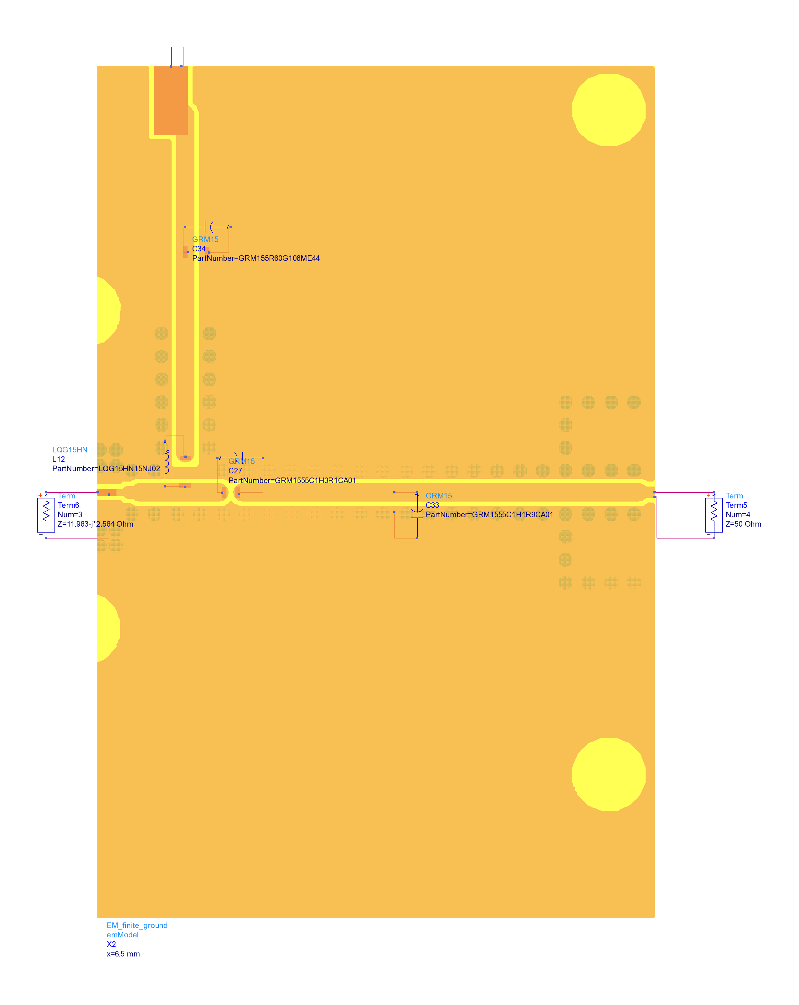
I set cond1(pink) as the top metal,and cond2(yellow) as the bottom metal. Because I use CPWG, the holes are placed to connect the cond1 with cond2.
Is it right for finite ground plane?
For the port setup, I've tried two ways
1. I set all the pins as global ports:

2. I set (Pin1,10),(Pin2,11),(Pin3,13) as three differential ports,and other pins remain global ports.
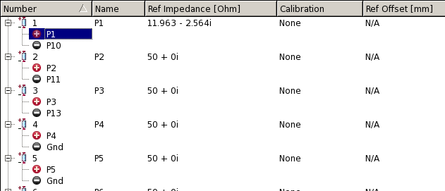
But the results are different, I don't know why....
Could anyone give me some advice?
Thanks~~
Have you connected the ground plane to the global ground then? Ask yourself: Where does return current flow, through the ideal ground connection or through the longer physical path in your model?
Hi Volker,thank you for your reply.
What do you mean to connect the ground plane to the global ground?
Because my substrate doesn't have infinite ground plane,
I remember that Momentum can handle this case by using “ground at infinity” as a reference when I set all the ports as global ports.
I meant the connection at schematic level, if your port reference is global ground (ground at infinity). If your EM model has a finite ground, but you don't use them in the Port editor, then no current will flow through the finite ground, and it might even be floating (-> capacitance line to GND) if you don't connect it in your schematic. Mixing global ground pins and explicit ground pins can create models that have a different current path than you expect/want. Easy to make mistakes there. Please show your schematics for the two cases that you compare.
The schematics and layouts of the two way I've tried are the same.
layout

schematic

The difference between them are the port set up.
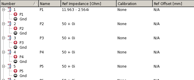

P1(@top layer),P10(@bottom layer) are both area pins where are the drain of the transistor.
P2(@top layer),P11(@bottom layer) are pins where are the SMA connector.
P3(@top layer),P13(@bottom layer) are both area pins where are the DC input power.
Other ports are used to be Murata SMD pads,and I leave them as global ports in both two ways.
By the way, I don't know if I put the negative pin (P10,11,13) at the bottom layer or at the two guide line of CPWG on the top layer, to fit more closely to the real return current flow.
Thanks for your reply~
I see ... with single ended Momentum ports, you connect them differentially in the schematic. That should work.
Looking at your screenshots, I don't see what is causing the difference. The one issue that I see with both cases is that shunt parasitics in the SMD elements are connected to ADS global ground, but that global ground is not connected to your PCB/port ground.
Hi volker:
1.I've found out the mistake.
Attachment 121751
This is the infinite ground plane case.Because I want to sweep the location of the pin(P8) which is used to connect the shunt capacitor, I use two MLIN components in the layout with component parameter x to be sweep, but I forgot to check the substrate of MLIN.
Attachment 121750
When I replace MLIN component with rectangles, the results of the two cases we discussed get closer.
global port setup:
Attachment 121753
differential port setup:
Attachment 121754
But the S11 still can't match completely together, is this acceptable?
2.
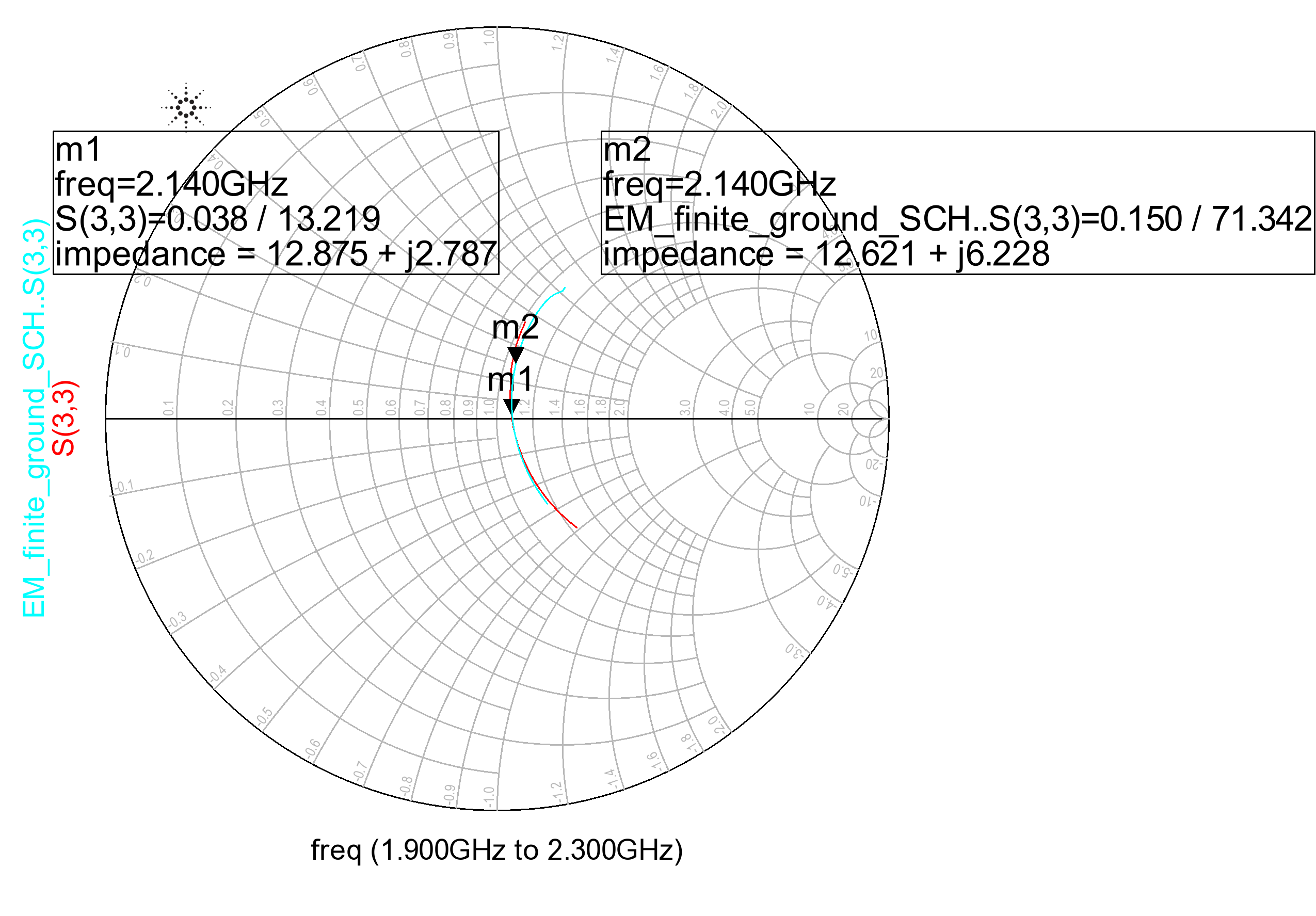
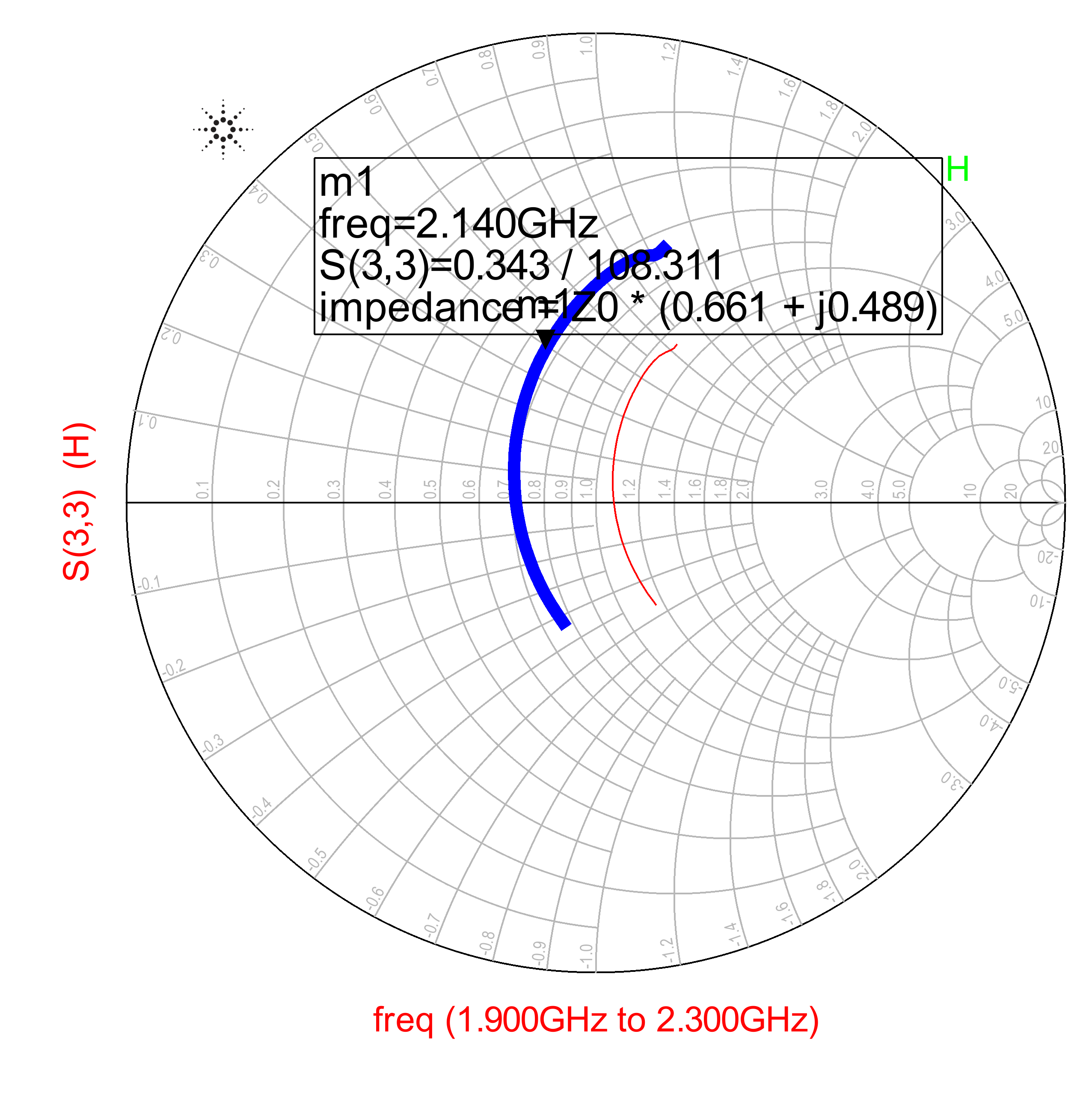
The result above is the comparasion of infinite ground case(red curve,m1) and finite ground case(blue curve,m2)
Does it make sense?
3.I have found another big problem.
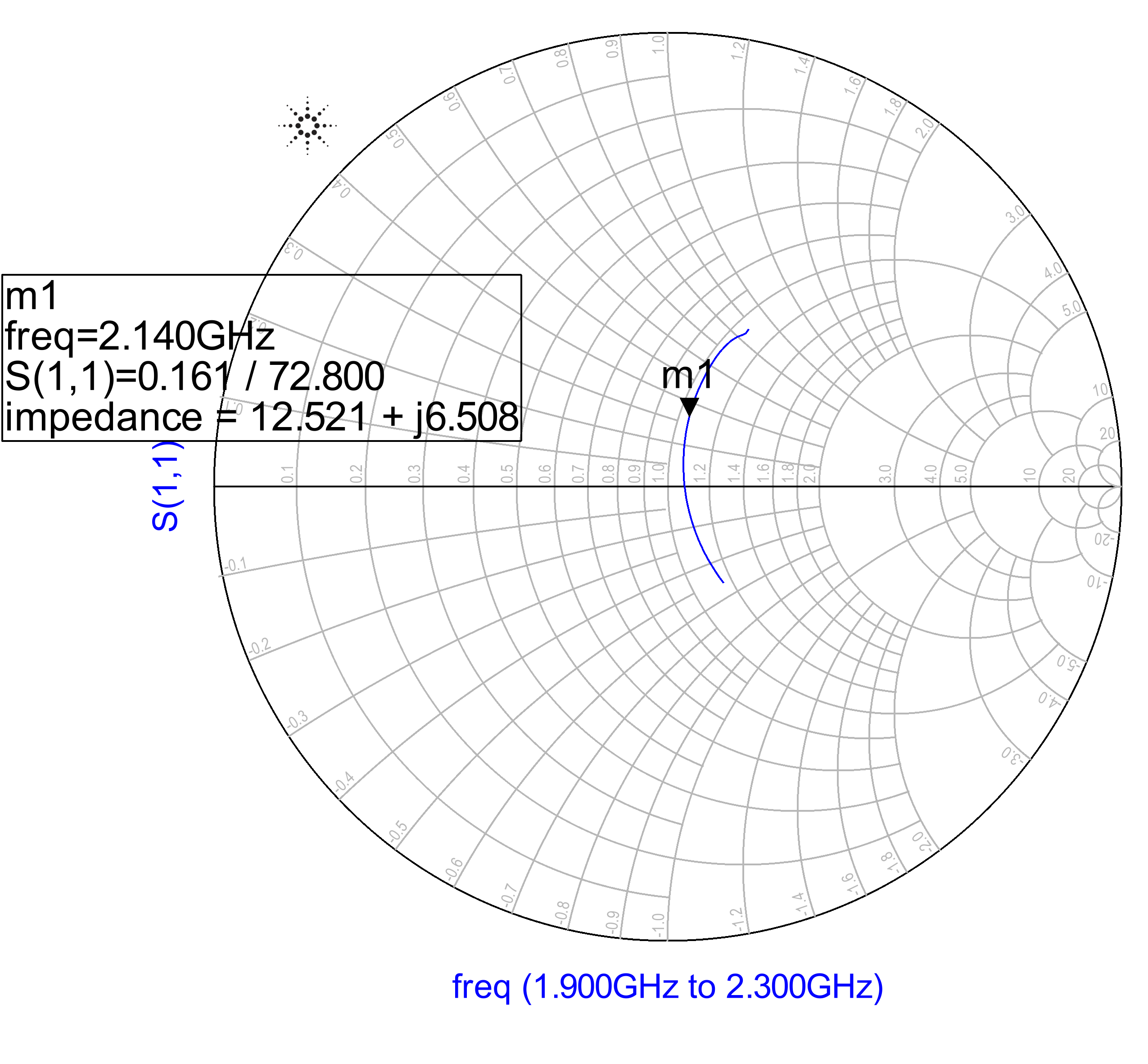
When I change the frequency type from adaptive(1.9GHz~2.3GHz) to single(2.14GHz) in the em setup,the results can't match the original results:
global port setup:
Attachment 121756
differential port setup:
Attachment 121757
I am not sure what's the accurate result...
Jeff, your attachement links don't work.
Hi volker:
1.I've found out the mistake.
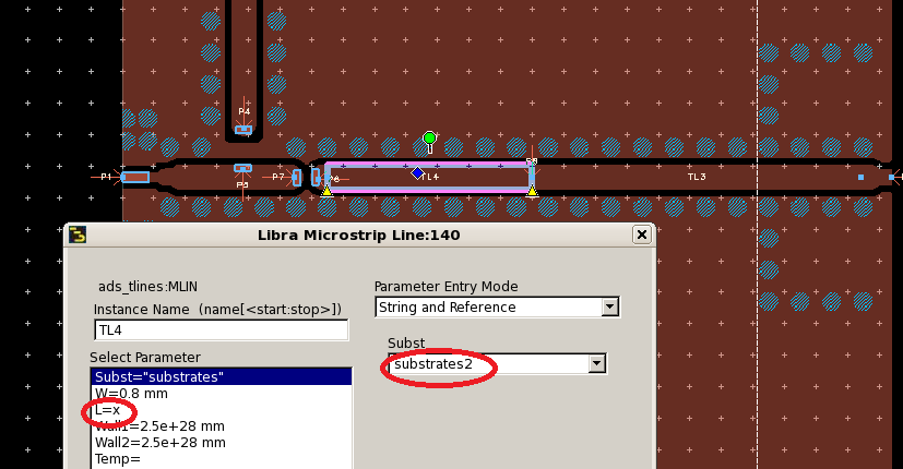
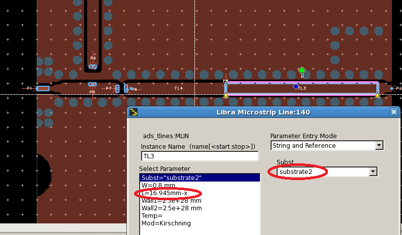
This is the infinite ground plane case.Because I want to sweep the location of the pin(P8) which is used to connect the shunt capacitor in the em-cosimulation, I used two MLIN components in the layout with component parameter x to be swept, but when in the finite ground plane case, I forgot to change the substrate of MLIN to the finite ground one.
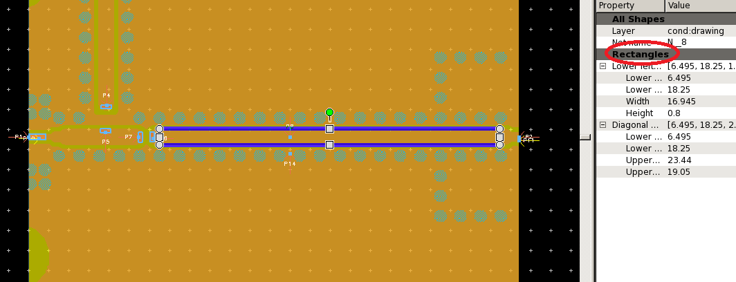
When I replace MLIN component with rectangles, the results of the global port and differential port get closer.
global port result:

differential port result:
But the S11 of both still can't match completely, is this acceptable?why?
2.

The result above is the comparasion of infinite ground plane case(red curve,m1) and finite ground plane case(blue curve,m2)
Does it make sense?
3.I have found another big problem.
When I change the frequency type from adaptive(1.9GHz~2.3GHz,npts 41) to single(2.14GHz) in the em setup,the results can't match the original results:
global port setup:
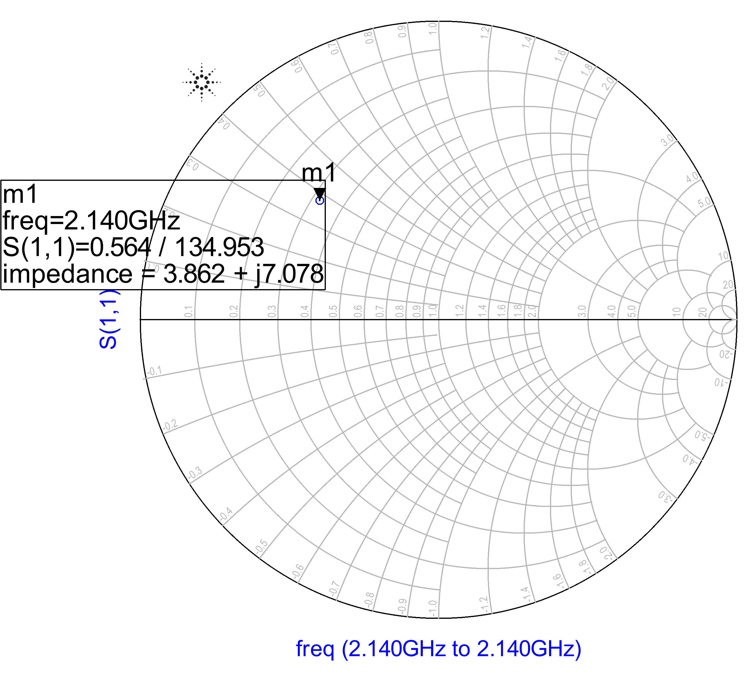
differential port setup:
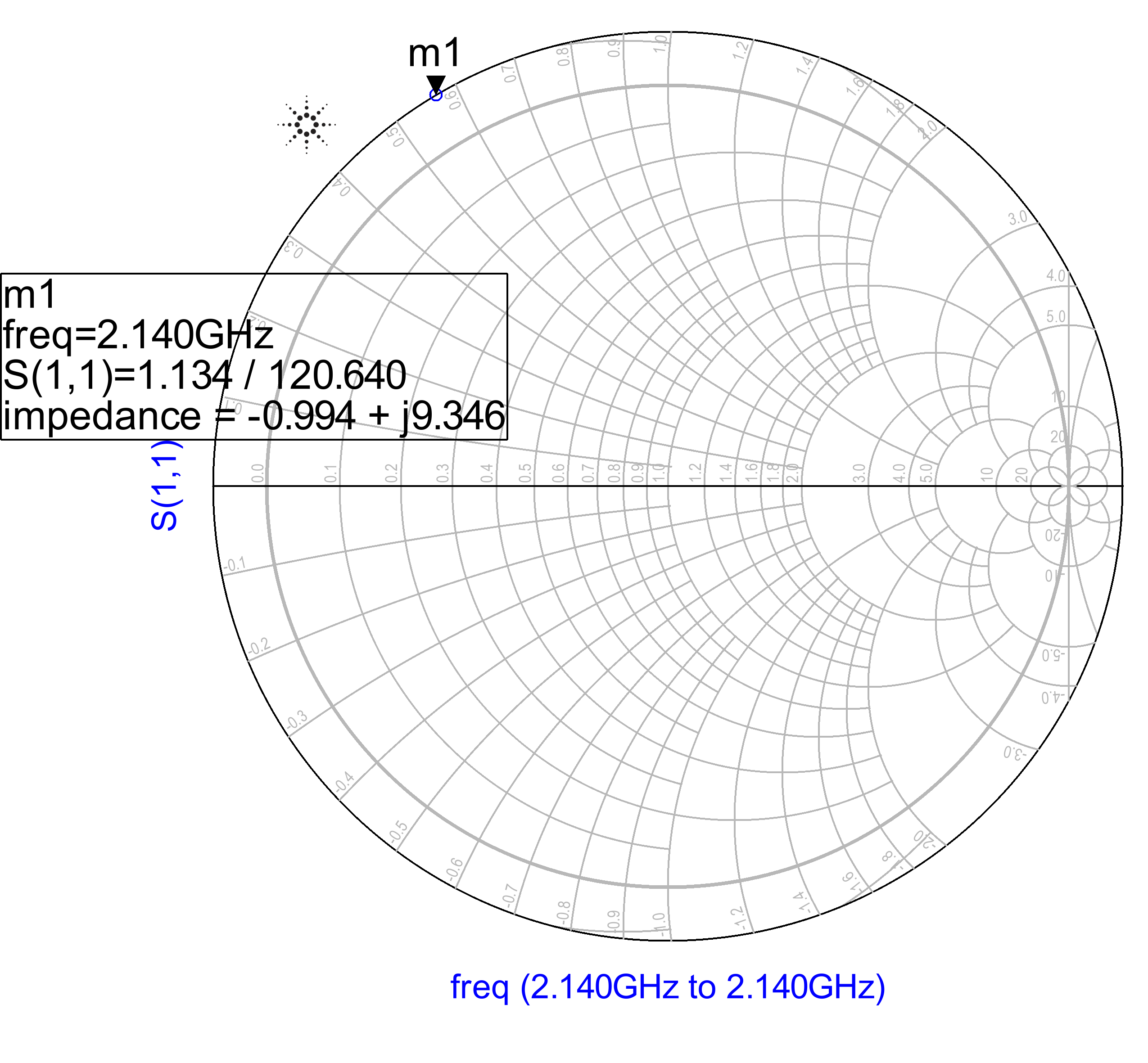
I don't know which is the accurate result...
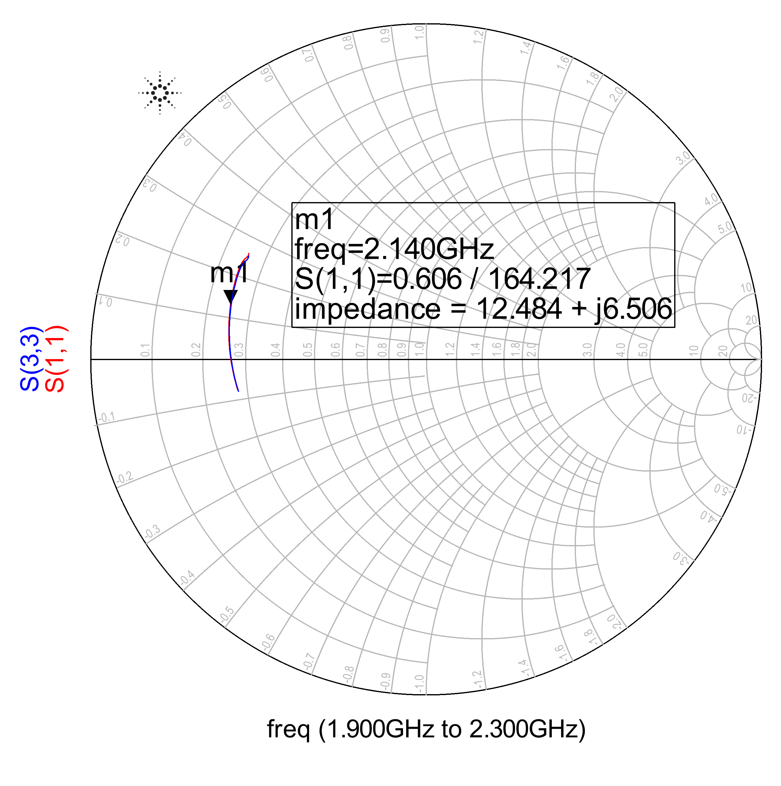
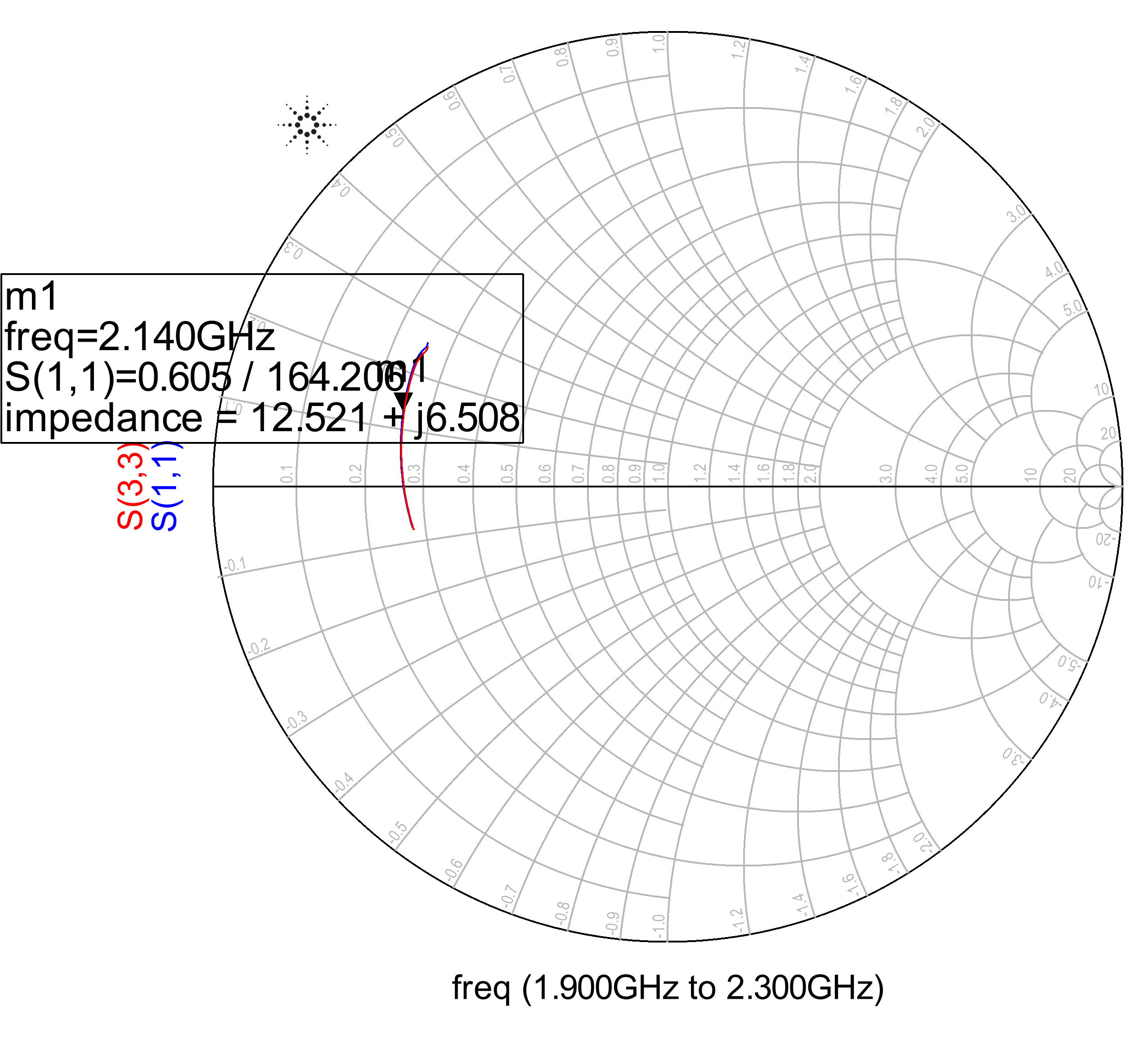
I have found the answer to my problem.
When I change the impedance of the port 1 from 11.963-j*2.564 Ohm to 50 Ohm,
the results of linear and adaptive match together.
But I don't know why the complex impedance of the port will cause the mismatch.
The result of differential and global still can't match completely.
global port(adaptive and linear):
differential port(adaptive and linear):
Thank you volker. You really helped me a lot.
