Ground Plane - Rectifier
时间:04-04
整理:3721RD
点击:
Silly question here,
I designed a rectifier and an impedance matching network for RF energy harvesting.
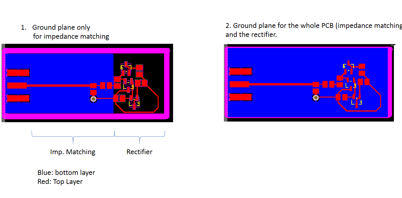
The impedance matching network needs a ground plane in the bottom layer. Currently, this ground plane is only behind the matching network. If I extend it to be under the rectifier section, will this layer affect the performance of the rectifier?
Best Regards,
Sebastian.
Here it's what i mean.
Thanks.
This is the schematic, hope you can help me.
Would be like this schematic, but whit a different Impedance mathching network. My Mistake...
I designed a rectifier and an impedance matching network for RF energy harvesting.
The impedance matching network needs a ground plane in the bottom layer. Currently, this ground plane is only behind the matching network. If I extend it to be under the rectifier section, will this layer affect the performance of the rectifier?
Best Regards,
Sebastian.
Draw a sketch and lets see..
Here it's what i mean.
Thanks.
Your layout is not a proper layout for RF systems.If you can draw the schematic, I can help you more..

This is the schematic, hope you can help me.
Would be like this schematic, but whit a different Impedance mathching network. My Mistake...
You don't have to cover around the SMD components on TOP side.Place the SMD component properly ( short distances,not too close,not too far,symmetric) and supply GND connections for the components which are needed for and supply multiple GND vias to BOTTOM GND layer.TOP layer GND has not be around the components.Instead move the TOP GND from TL if you don't use CPWG.