RF PCB antenna design in PCB
时间:04-04
整理:3721RD
点击:
Hi All,
In PCB antenna, say inverted F antenna's one end is connected to ground.
It literally means we are shorting the TX or RX signal to ground.
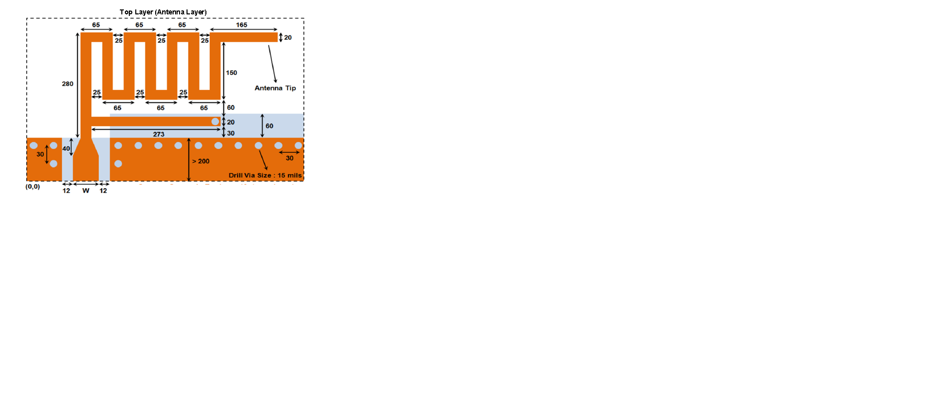
Can anyone please explain why we are shorting the signal to ground?(As in image attached)
Thanks in Advance.
Arun
In PCB antenna, say inverted F antenna's one end is connected to ground.
It literally means we are shorting the TX or RX signal to ground.
Can anyone please explain why we are shorting the signal to ground?(As in image attached)
Thanks in Advance.
Arun
no arunmaran10 it is not like that. In microwaves electrical connection to ground doesn't mean actual grounding. Actual grounding requires via fillings all over the pcb and not just in one or two positions. In inverted F shorting is used in order to shorter the current path and in other words to decrease the resonance frequency without increasing the dimension of the antenna. That is the resonant dimension would be lambda/4 instead of lambda/2.
The inverted F "short" can be understood as a matching network using transmission line stubs. I'm not sure if the shown example is actually working, it looks way different than usual inverted F designs.