Metal patterns in PCBs
时间:04-03
整理:3721RD
点击:
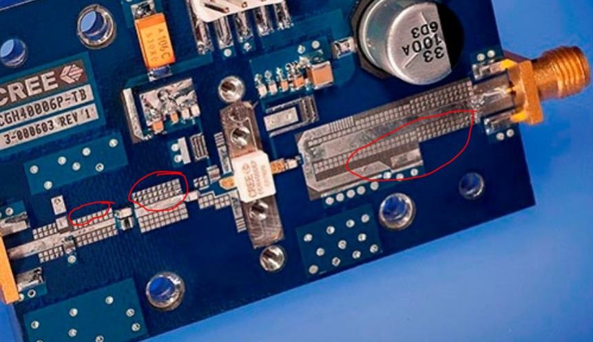
I ran in to this picture of a pcb in a datasheet. It was just weird for me to see this metal pattern on the top layer. Any thoughts on why this exists?

I believe it's a PCB waveguide.
No..It's a pattern to tune the Matching Circuit.
How can you tune the matching circuit? The copper squares surround the microstrip, and are not tunable.
Could it be a metal filling rule? something like on-chip design rules?
They are just to connect a SMD component where the matching is proper.The designer may make a fine tuning to shift left and right the matching component.
There are also stub optional pads around it.They are for to tune the length of the stub too..
栏目分类
