[Moved]: RF 50 ohm PCB trace width
I'm using a few different microstrip calculators, but when I draw my trace, the suggested width (2.77mm) seems huge.
Calculator here: http://www.rfdh.com/
The transmission line needs to be 50 ohms as it connects directly with a 50 ohm matched impedance IC, of which the leads are around 0.3mm or even smaller.
I'm using FR4 and this is a 2-layer board
dielectric constant er is 4.5
Frequency of operation (3 to 6 GHz)
strip thickness is 1 oz copper, 0.035mm
dielectric height is a standard 2 layer board, it is 1.6mm
I need a Z0 of 50 ohms transmission line.
What am I doing wrong?
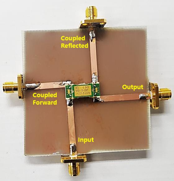
I recently fabricated a directional coupler, to be used in my system. I kept 2.77mm width and it did not give me good results, results are very strange.
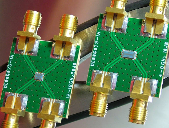
And I googled some directional coupler PCBs and their evaluation boards, they under 4-8GHz are using a very thin trace. How the width became so thin/narrow if that also is a 50 ohm tx line?
I am attaching my fabricated directional coupler and also the Google samples.
Please see my fabricated directional coupler with 2.77mm (50ohm) trace width below:

and the googled directional coupler samples are:

Need an advise on how can I make a thinner/narrower 50ohm width to fabricate my directional coupler with minimum losses.
Thanks!
Hi, For the PCB thickness you have this is correct the microstrip will be wide. You can should reduce this to a thinner PCB such as 0.8mm. This will equate to about 1.4mm for 50ohm trace. Hope this helps...
2.7mm is correct for 1.5mm FR4, but be careful with discontinuities at the connectors. Also, standard FR4 is very lossy at GHz frequencies. For your 3-6GHz PCB, better use RO4003 or another low loss substrate. Or at least use thin FR4, if you can afford the losses. This will also help with the step in width at the SMA connectors.
Line impedance is approximately Zline=sqrt(L'/C') where L' is inductance per unit length, and C' is capacitance per unit length.
For smaller trace width, you need to increase the capacitance to ground. This can be a smaller substrate thickness, or additional ground on the sides as in your example. The side ground is connected to bottom ground with via fences, and increases the capacitance.
Also, GND connections of SMA connectors don't seem to me well tied.I hope you did simply not solder the bodies to GND plane..
FR4 is not a appropriate substrate for 3GHz and beyond.
Hi, fr4 is fine upto 6GHz. I have implemented many antennas on standard fr4 with minimal loss and dual WiFi antenna with efficiency upto 70/80%.
That really depends on the antenna type. PIFA will be ok, patch antennas suffer from the substrate losses.
Hi, the antenna is not the feed. If the feed is still designed and for instance at GPS 1575.42MHz for a ceramic patch. Then the patch will be fine. I see no issues here providing the design of the feed is correct. It's very common for patches to be placed on Fr4.
Your post was misleading. You wrote that you implemented antennas on FR4, and my understanding was that the antenna itself is a PCB antenna. Of course, if you just place ceramic antennas on FR4, the antenna performance will be fine and FR4 only affects the feed line loss.
I agree.
Coming back to the initial post: I wouldn't use FR4 in the 3-6GHz range mentioned there, but it is possible when the extra loss is acceptable. Design for appropriate line width, simulate loss and decide if it's acceptable.
