Simulating 4-Layer PCB with microtrip Antenna- Help-
时间:03-30
整理:3721RD
点击:
Hello guys,
I am beginner, about simulate on CST MWS and EM topics.
Well, let me explain.
I have four models of microstrip antennas GSM dual band. I simulated each one with the same conditions, PCB size and thickness for copper and FR4 respectively, discret port (S-parameters) , Open space, and under ideal conditions.
After that, I choice the better one, I designed the PCB on Altium and added the Antenna.
But, the PCB is designed on 4 layer.
Now I am trying of simulated the PCB, imported with EDA but under conditions for planar antenna on CST MWS.
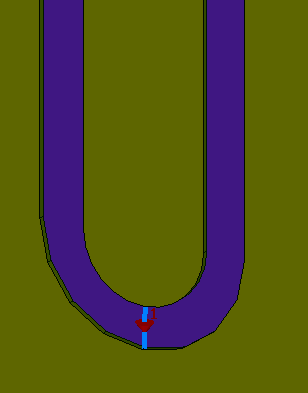
I achieved reduce the mesh below one million. But, I placed my discrete port between my module pad (Antenna signal) and surrounding ground. For me that was logical, but
I have the doubts if I placed wrong the port and if now for a complete PCB with more signals and planes the antenna it isn't the better one.
Could you please give me an advice? Thank you.
I am beginner, about simulate on CST MWS and EM topics.
Well, let me explain.
I have four models of microstrip antennas GSM dual band. I simulated each one with the same conditions, PCB size and thickness for copper and FR4 respectively, discret port (S-parameters) , Open space, and under ideal conditions.
After that, I choice the better one, I designed the PCB on Altium and added the Antenna.
But, the PCB is designed on 4 layer.
Now I am trying of simulated the PCB, imported with EDA but under conditions for planar antenna on CST MWS.
I achieved reduce the mesh below one million. But, I placed my discrete port between my module pad (Antenna signal) and surrounding ground. For me that was logical, but
I have the doubts if I placed wrong the port and if now for a complete PCB with more signals and planes the antenna it isn't the better one.
Could you please give me an advice? Thank you.