How can i design defected ground structure in AWR ?
时间:03-29
整理:3721RD
点击:
Hello
I want to design a defected ground structure (dgs) in AWR,
i don't know where i set the ground layer and how to set the boundary
plaese help me
I want to design a defected ground structure (dgs) in AWR,
i don't know where i set the ground layer and how to set the boundary
plaese help me
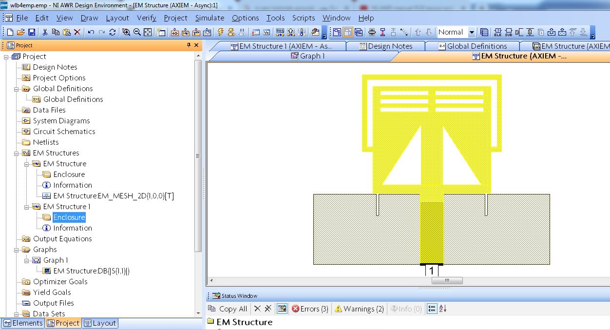
Arrange the layers and associated materials and other stuffs in "Enclosure" box and make the "Bottom Boundry" being as Open.
Then connect the Ports in according to this new arrangements..Ports should be connected to "Bottom Additional Layer"
Thank you for your answer, please can you explain by pictures or give me a Tutorial cause a im not very familiar with this sofware,
thank you BigBoss,
Thank you BigBoss for your quick answer, please can you explain with pictures or give me a tutorial link cause i am not very familar with this sofware,

栏目分类