Advanced Design System - Stripline Calculation
I try to design my second PCB with Keysight Advanced Design System (the first PCB was just a 50 ohm microstrip) and Im looking for a how-to or something else. The plan is to measure three components in series. Now, im looking for an idea to calculate the microstrip transmission lines.
My first idea was to calculate the entire transmission line (with 50 ohm termination at the beginning and end of the stripline) and optimize the length and width of the elements with some goals (minimum reflection coefficient within 700 MHz and 2.5 GHz and special focus to 2 GHz).
The three shorted s2p containers are my elements of interest, the tee's are necessary in a later part of the design but not important at the moment. The results are shown in the next picture:
After that, i activated my s2p containers (all three elements are real inductors with an inductance of 13 nH) and simulated again.
I've got a capacity at 2 GHz, that's not what I want (I know, at high frequencies changes the inductance to a capacity, but there must be some design hints to avoid that problem). I expected an inductance about 40 nH as seen in the next picture (simulation with 3 inductors in series just optimal with wires between).
My question is: what is the usual way to design a stripline for that simple board? Should I optimize the stripline before every s2p container (second term element after the s2p container) with the goal of minimum transformation caused by the stripline? Or should I optimize all striplines at once (term at start and end of the stripline) with the goal to match my results with the expected reflecion coefficient in the third picture? Are there any design rules I have to observe?
The bottom layer of my PCB is a ground plane. On the top layer is just the transmission line without any ground. Is it necessary to add a ground plane on the top? Maybe for better results of my transmission line (i have no idea how to add a ground plane on the top)?
Thanks for your help!
It will be a easier if you assemble your circuit from 50 Ohm blocks, and match each block separately.
You mean side ground on the same layer as the "signal" conductor? That would be grounded coplanar. You can do that to have better shielding between adjacent lines, and reduce line width, but it's more difficult to model. Microstrip (just bottom ground) is easier and you can use the predefined circuit models in ADS, so I would start from there.
Good morning Mr. Muehlhaus and thank you very much for your response.
Okay, i'll start with only ground at the bottom layer. It was just a question if there are maybe some clear advantages with a ground plane at bottom and top compared to only ground at the bottom layer.
Today, I started with assembling 50 ohm blocks. But I have already first issues with the connection from the input-stripline to my device. The first microstrip should be have a minimum width of 1mm and a minimum length of 5mm (dimensions of the SMA connector). The width of the second stripline should be 2.6mm (size of the inductor package). I figured out, that i get a better match with a step in width discontinuity between the small and big stripline instead of using a taper (picture1, first post). I used goals and optimization again for the best match.

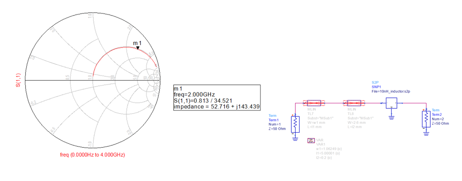
At the second picture is the inductor without any stripline. That's the smith chart that I want.

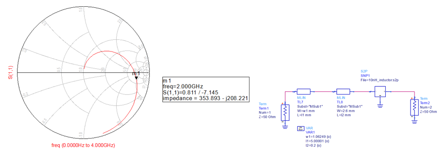
But in combination, I've got a capacity at 2 GHz again even though I used a 50 ohm stripline.

What i'm doing wrong? I think it's just a simple failure..
mhmm.. okay. I think the length of the transmission line causes a rotation around the middle. how can I compensate this effect?
Yes, that is what a transmission line does. Compensate line length - what for ?
Your entire task and workflow is unclear. It will be easist if you described what you are trying to do - what are your S2P blocks and what circuit are you building, and what is the purpose of the lines and tapers in your design? Are the lines for circuit functionality, or just model the connection of a semi-lumped element ciruit? And why do you simulate with the S2P replaced by thru?
Hi,
I want to measure (with networkanalyzer) 3 inductors in series configuration.
At first, I try to simulate the stripline just for one inductor.. In the s2p blocks are the files of the manufacturer (of the inductors i want to measure).
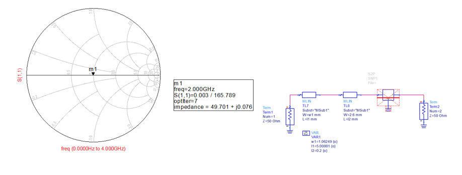
Okay, the first picture in my last post was only a simulation of my stripline (without the inductors s2p file) to check my 50 ohm transmission line. The second picture was the simulation of the inductor without any transmission line and the third one shows the combination of both.
The transmission line causes a rotation of the inductance around the middle (dependent of the length of the transmission line). The result is, that I measure a capacitance at the output of the inductor on the basis of the rotation.
I know, in the other thread is a very similar discussion about shifting the calibration plan or a calibration direct at the port of my DUT. But what if i need an exactly impedance of 10nH for example at the output of inductor? The final goal is not to measure the exactly impedance of the inductor, I want to create a matching network that I simulated before with ideal components (the tee's in my first post, first pictures are later for capacitors). I hoped to get a fairly match between the simulation with real and ideal components. For that reason, I try to compensate the transmission line's rotation to get the right impedance at every point in my schematic that I want (inductors and capacitors are lumped elements).
Or is that a bad/impossible idea?
