4 Layer stackup filter response help needed
My question is detailed one i hope to get some valuable response.
I have designed a bandpass filter and want to see its response on 4 multilayer stackup (Top, gnd, pwr, bot) on ADS 2014.
I have few issues that i want to clear.
1) I simulated BPF alone and its response is correct when there is complete ground plane. (signal, dielectric, gnd)
2) When i changed the ground plane of BPF to aligned it with top layer of multilayer stackup its results are changed. Can anyone tell me how i can achieve correct results as i get it with complete ground plane beneath.?
3) I aligned my BPF (sig, dielectric, gnd) with 4 layer stackup (top, gnd, pwr, bot) and simulated the whole and its results were again changed from previous one.
I have attached substrate description aswell.
How did you configure the Portsin according within new layout ?
What i did was i aligned my BPF on 4 layer stack. I have attached picture of port description aswell its direct
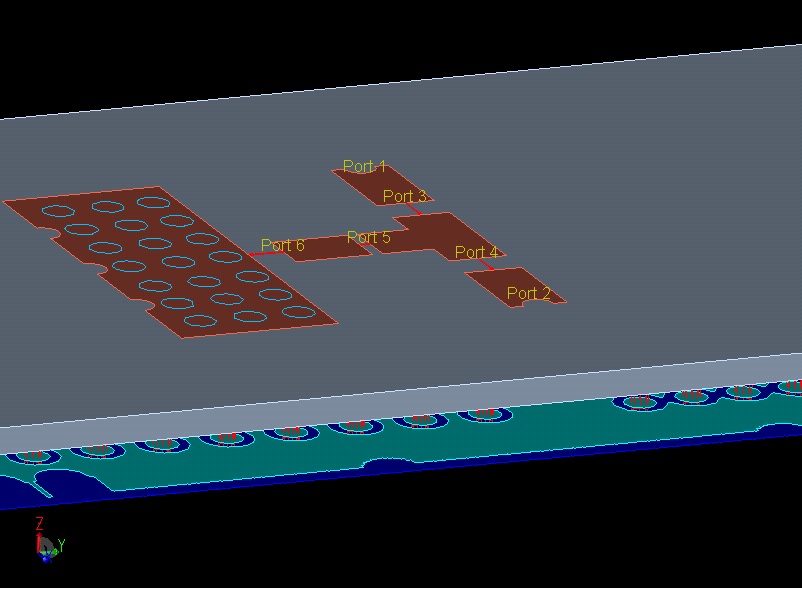

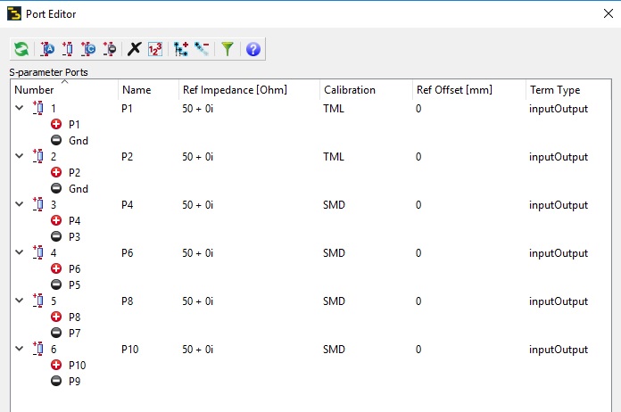
P1 and P2 have a GND reference but that GND does not exist just underneath of the Ports.In this case, where the ports' currents will return back ?
They have GND layer reference but this reference is floating.This won't work..
You should consider the Ports being as Generators and they have to have a GND return path in any case.
Also, SMD calibration is valid only if and if SMD components have no GND return path in their equivalent circuit/models otherwise this will also create a trouble..
I agree, this use of ports is not approriate. You need port references at the ground layer, instead of placing "floating" SMD ports. The issue with "floating" SMD ports is that they don't allow any shunt path currents.
In ADS 2017, there is a new setting where you can select a layer for the ground reference. This is the slide from my EM training on that new feature:
Thankyou so much for the response.
I got the point of GND reference part that you mentioned.
i simulate my filter individually (sig, sub, gnd) and i don't require complete ground beneath rather a different.
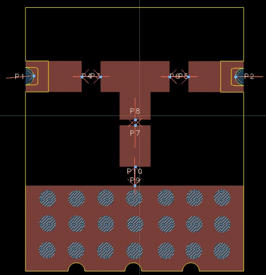
i made cond2 as a ground now and made a hole so that GND reference should get return path in this case. Am i doing it correctly?
Also kindly let me know should i use TML for lumped elements in my case or SMD?
i have attached screenshots aswell.
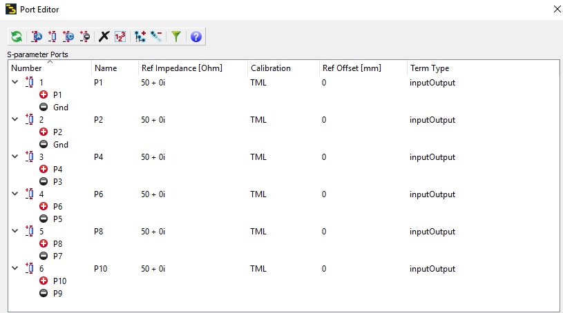
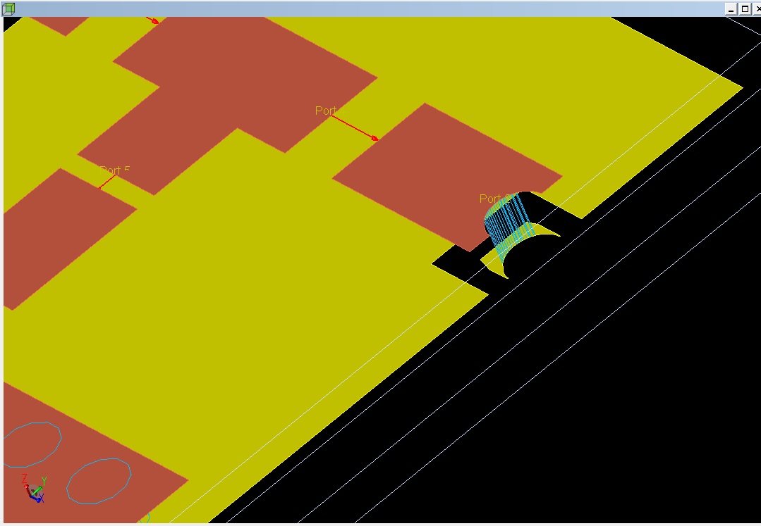
SMD is not accurate for component data that includes shunt effects.
You can't use normal TML here because there is no space for the cal standards.
I would use Calibration "None" or "Zero length TML".
Another problem is your P10 (or P9?) at the large ground. Move the pin a little bit inside the metal area, instead of placing it on the edge. Otherwise the port will cover the complete edge of the ground plane, resulting in wrong port currents. http://muehlhaus.com/support/ads-app...edge-area-pins
I would check in EM preview window to see where the port connects to on both ends.
Thankyou for your kind response,
I am using SMD here because i want to apply parametric sweep in co simulation after making them symbol. The reason i chose SMD bcz capacitor i want to attach is in series with two traces. I hope you understand and i am doing it right.
Actually i am not getting my starting point bcz first i need to achieve correct HPF response of single layer then i will stack it on 4 layer PCB.
With complete cover beneath gives correct and as soon as i give required ground beneath its results starts to differ.
I understood what you are trying to do. Read my answers again. Good luck!
Best regards,
Volker
(Keysight Certified Expert EDA)
