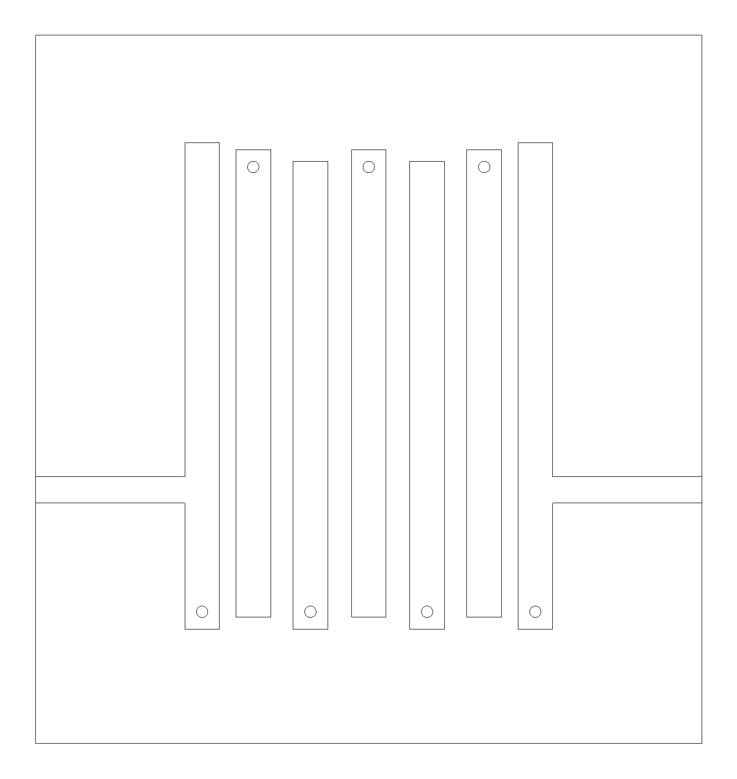
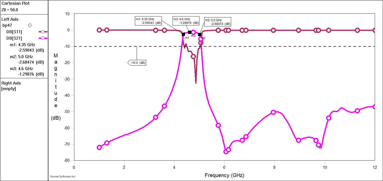
Verification of a 3D simulation of a bandpass filter
The filter was checked with 3D simulations (CST).
I would be very interested in verifying the simulations with other tools (HFSS, ADS, Sonnet,...).
If someone has the time and the desire, I will provide the layout and the necessary information
for the simulations (Gerberfile). After manufacturing and measuring the filter I will present
the results in comparison. Who wants to try?

Substrate: h=0.254 mm,
Frequency range: 1-12 GHz
Having worked in EM simulation for 20 years, I have seen many measured-vs-simulated comparisons.
You get a bunch of curves, but these are usually difficult to interpret because of manufacturing effects (etching tolerance etc), measurement tolerances (port calibration), uncertainties in the material modelling (rolled vs. electroplated copper, inhomogenities and anisotropy in woven substrate) and user related simulation inaccuracies. In addition, the boundary conditions (side walls and top cover vs. open) matter.
So what is the purpose of your testcase? Public benchmarking is usually prohibited by the software license agreement. If you just need a second opinion on your simulation, we need geometries and more complete material data.
Here are some more infos and a gerber file with the top-layer data. I know the problems of comparing measurements and simulations from my own experience. Nevertheless, I would be interested to know how far away the results are.
Your gerber file is not correct. It seems that you have all layers in one file (or just the ground plane width drills?). Gerber requires one file for each layer. You better use DXF instead, and please import yourself to check that it's complete.
Thanks for trying. Now only the top layer in the Gerber file.
Quick check

Ok, I can add some FDTD results from Empire XPU. At the moment, I use that for RFIC on-chip antenna simulation mostly (240GHz on-chip antenna etc) so hopefully there's no user mistakes for this PCB use.
Model details:
Substrate er=3.66, tand=4e-3
Conductor copper for top metal, PEC boundary for bottom side
Side walls absorbing sheet, top cover PML6
Microstrip ports
Mesh setting "very fine", 1.5MCells
For comparison to measured, we should check the influence of via position offset. What do you think,is +/-100 μm reasonable?
A quick test shows that via hole placement is indeed very sensitive. This is what we get with via displacement (all vias same offset) of x=50μm, y=50μm and x=100μm, y=100μm:
Thank you for the simulations! The results are not far from my simulations. If possible and allowed, please save the S-parameter file (Touchstone format xx.s2p), so I will summarize all curves in one plot.
I prefer not to do that, because everyone here uses slightly different model settings and such a comparison can be misunderstood by readers as a tool accuracy benchmark.
