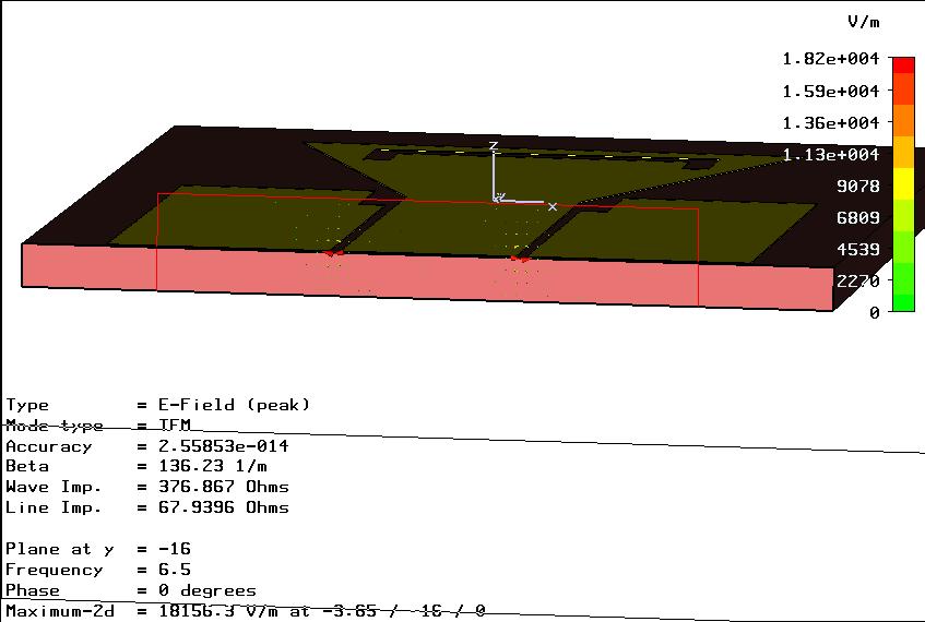
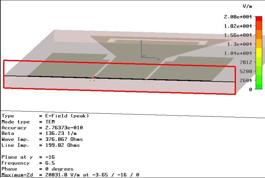
cpw 50ohm
i noticed the quite different calculated Line Impedance is obtained for ports with different width.


BTW, what does the following warning mean: "The degeneration of TEM modes at the homogeneous port 1 could lead to undetermined modepatterns. It might be suitable to define a multipin port instead" and what is its influence to the results?
width: about 3*(2g+s)
height:about (3-5)*h
odd mode and even mode can be excited, but it doesnot matter, only the results for even mode are needed.
hi Burton and DrunkBear,
This formula is exact in HFSS. However in CST, It's better to use another one as:
For CPW:
Port_width = 3 * (2G + S)
Port_height = 2G + S

And for G_CPW:
Port_width = 3 * (2G + S)
Port_height = h + 0.5*(2G + S)

Thanks for both!
And nhomuathu_hanoi, it seems G and s have not been defined and shown in the picture offered, could you pls further explain them?
HI
I agree with DrunkBear, so I think, the width of port should not so big!
Then, if we use a ground with transmission line, should we make the CPW port over the ground (look like Ungrounded CPW port defined by nhomuathu_hanoi), or it just only touches the ground as in the second image of DrunkBear ?
To DrunkBear, the line Impedance varies a lot with respect to the width of port, so should we need to reduce the port width to meet 50 Ohm Line Impedance (as seen in your images, the Line impedance decrease as reducing the port width)?
Last, what is s,g in your formulas? (h is the thickness of substrate)
thanks,Regards
I my opinion the with and height of CPW depends upon the choice of frequency rage, higher the frequency lower the width and height of port. A good idea is to adjust the port dimension near 50ohm.
hi khangkhang
s is the width of the centre strip line and g is the gap between the centre strip and the outer ground strips
i hope this clears your confusion
regards
Thanks shahid78,
It seems that g does not exist in my structure
(picture)
then, how can I apply such those formulas above?
regards

Added after 1 minutes:
my structure is using a vertical ground plane, as seen, its one side is ground (below side in the picture)
thanks for your help!
Added after 13 minutes:
(CST) in my design,
the width of used Transmission Line is only 1.2 mm, and the substrate thickness is only 0.5mm, so the Waveguide port for my case is seen to be very small compared with the 50x80 mm ground plane !?
Last, if we use the discrete port, we don't pay attention in setting, but, what is the different of them?
Regards,
Added after 6 minutes:
to snkhan:
i have tried to adjust the port size to 50ohm, but it seems not easy!
Assume if we can not adjust the port size to meet 50 ohm, but we can use the Z-normalize with seeting of 50 ohm, and the S11 is also reliable, is it right?
regards

well it seems you have microstrip line and not CPW line
in that case you should use 6----10*w as your port width and 5*h as port height where w is the strip width and h is the substrate thickness
i hope this helps
regards
thanks shahid78,
then I should define the waveguide port for my microtrip line that just only touch the ground (like of DrunkBear) of over the ground (like of nhomuathu_hanoi)
regards,
Hi KhangKhang
Some how u have to manage around 50ohm while changing the width, height etc. In my option as far as CST is concern, to normalize to 50ohm would be technically sound but not good enough.
As an example if u normalize to 50ohm and if u manage to get port around 50ohm will give you different results.
thank you snkhan,
I have tested and seen it right!
Actually, when we use a "full plane" wave guide port, we have a Line impedance near of 50 ohm, however, the radiation and total efficiency is very low (only less than 20%)! It is found that these efficiency would be raised with the reducing of port, and the Line impedance is reduced as a results!
Any idea?
Added after 3 hours 12 minutes:
Hi all,
with CST, the simulations in different versions will give different results, is it right?
I checked with the same structure, and same every setting condition, the Line impedances are quite different, i.e, the line impedance in the older version is nearer 50 ohm than the newer one.
Anyway, we should believe the results in the new version, am I right? I know the mesh generation mechanism is usually better in the new version, but the different should be acceptable!
Now, i am trying to get port around 50 ohm value, but it is not easy!
Please have a glance on my design (above). If I use open (add space) in all direction, the simulation become unstable (energy not be converged). Then I used only open boundary at the port location (end of the ground), the simulation is stable, but the far field is noticed is unaccuracy at some low frequencies!
Thanks for your helps!
Added after 46 minutes:


hi khangkhang
well you should use port height such that it just touches the ground plane but not covered the ground
regards
Yes u r right. In CSt u need to have same boundries for stable radiation pattern.
Hi everyone,
I have a problem. I am simulating a FSS cell in CST Studio and I want to calculate the reflection coefficient in a frequency range with a plane wave (TEM mode). I am using a waveguide, but I am not sure which mode I am exciting with a waveguide. Any of you can you tell me how to excite a TEM mode with a waveguide port.
Thanks in advance,
David
Using the rules of CPW for waveguide port, CST reports that waveguide port is too short. Increasing the mesh density does not help either
