关于一个设计里面rst连接了同步复位和异步复位的DC约束问题
基本描述:top的rst引脚连接了五花八门的reg,同步复位、异步复位和同步置数,综合脚本对rst设置了ideal属性,经过长达12小时的综合过程后输入路径仍然有高达1300+的时延,critical path始点为rst,终点为某一同步复位reg的reset端。

问题1:由于已经对rst设置了ideal属性,为何时序rst网络仍然有如此高的时延?
问题2:是否对于rst的同步路径,DC仍然做时序检查?(综合脚本对rst设置了input_delay和drive_cell)
附上综合脚本:
## Load design file
read_file -format vhdl "./src/pn_k16.vhd"
read_file -format vhdl "./src/pn_n16.vhd"
read_file -format vhdl "./src/mode.vhd"
read_file -format vhdl "./src/graycounter.vhd"
read_file -format vhdl "./src/T1/addr_ctrl.vhd"
read_file -format vhdl "./src/T1/output_ctrl.vhd"
read_file -format vhdl "./src/T1/accu.vhd"
read_file -format vhdl "./src/T3/rom_t3.vhd"
read_file -format vhdl "./src/T1/enc12_ram00.vhd"
read_file -format vhdl "./src/T1/enc12_ram01.vhd"
read_file -format vhdl "./src/T1/enc12_ram02.vhd"
read_file -format vhdl "./src/T1/enc23_ram00.vhd"
read_file -format vhdl "./src/T1/enc23_ram01.vhd"
read_file -format vhdl "./src/T1/enc23_ram02.vhd"
read_file -format vhdl "./src/T1/enc56_ram00.vhd"
read_file -format vhdl "./src/T1/enc56_ram01.vhd"
read_file -format vhdl "./src/T1/enc56_ram02.vhd"
read_file -format vhdl "./src/T1/ram_single.vhd"
read_file -format vhdl "./src/divider.vhd"
read_file -format vhdl "./src/mixer_16.vhd"
read_file -format vhdl "./src/asyn_fifo_reg.vhd"
read_file -format vhdl "./src/T1/ram_info.vhd"
read_file -format vhdl "./src/asyn_fifo_dpram.vhd"
read_file -format vhdl "./src/T1/enc_t1.vhd"
read_file -format vhdl "./src/T2/enc_t2.vhd"
read_file -format vhdl "./src/T3/enc_t3.vhd"
read_file -format vhdl "./src/combine.vhd"
read_file -format vhdl "./src/framer_16.vhd"
read_file -format vhdl "./src/enc_top.vhd"
current_design enc_top
link
check_design
## Define the global attributes for timing analysis
set INPUT_DELAY 0.5
set OUTPUT_DELAY 1.0
set CLK_PERIOD1 15
set CLK_PERIOD2 10
set CLK_UNCERTAINTY 1.5
set CLK_TRANSITION 0.3
set CLK_SRC_PORT [get_ports clk_src]
set CLK_ENC_PORT [get_ports clk_enc]
set CLK_OUT_PORT [get_ports clk_out]
## Set design constaint
set_max_fanout 20 [current_design]
# Set the max signal transition time for a net,
# as is written in this script, the nets of the
# whole design would specified.
set_max_transition 1.0 [current_design]
# Clock constraint
create_clock -period $CLK_PERIOD1 -waveform [list 0 7.5] -name sys_clk_src $CLK_SRC_PORT
create_clock -period $CLK_PERIOD2 -waveform [list 0 5] -name sys_clk_enc $CLK_ENC_PORT
create_clock -period $CLK_PERIOD2 -waveform [list 0 5] -name sys_clk_out $CLK_OUT_PORT
set_dont_use {scx2_tsmc_cl013g_ss_1p08v_125c/*LAT*}
set_dont_use {scx2_tsmc_cl013g_ss_1p08v_125c/SDFF* scx2_tsmc_cl013g_ss_1p08v_125c/SEDFF*}
set_dont_use {scx2_tsmc_cl013g_ff_1p32v_0c/*LAT*}
set_dont_use {scx2_tsmc_cl013g_ff_1p32v_0c/SDFF* scx2_tsmc_cl013g_ff_1p32v_0c/SEDFF*}
set_clock_uncertainty $CLK_UNCERTAINTY sys_clk_src
set_clock_transition$CLK_TRANSITIONsys_clk_src
set_clock_uncertainty $CLK_UNCERTAINTY sys_clk_enc
set_clock_transition$CLK_TRANSITIONsys_clk_enc
set_clock_uncertainty $CLK_UNCERTAINTY sys_clk_out
set_clock_transition$CLK_TRANSITIONsys_clk_out
# This command specify the net with particular drive resistance.
# The 0 value of drive resistance means the highest drive strength
# to the clock ports.
set_drive 0 [get_ports clk_src]
set_drive 0 [get_ports clk_enc]
set_drive 0 [get_ports clk_out]
set_dont_touch_network [get_clocks]
set_ideal_network [get_ports rst]
set_false_path -from [get_ports pat_*]
# set_false_path -from [get_clock sys_clk_src] -to [get_clock sys_clk_enc]
# set_false_path -from [get_clock sys_clk_src] -to [get_clock sys_clk_out]
# set_false_path -from [get_clock sys_clk_out] -to [get_clock sys_clk_src]
# set_false_path -from [get_clock sys_clk_enc] -to [get_clock sys_clk_src]
# set_false_path -from [get_clock sys_clk_enc] -to [get_clock sys_clk_out]
# set_false_path -from [get_clock sys_clk_out] -to [get_clock sys_clk_enc]
# set_dont_touch_network [get_ports rst]
set_driving_cell -lib_cell PDDW0204CDG -library tpd013nv3wc -pin C [get_ports din
set_driving_cell -lib_cell PDDW0204CDG -library tpd013nv3wc -pin C [get_ports pat_code
set_driving_cell -lib_cell PDDW0204CDG -library tpd013nv3wc -pin C [get_ports pat_disturb
set_driving_cell -lib_cell PDDW0204CDG -library tpd013nv3wc -pin C [get_ports pat_frame
set_driving_cell -lib_cell PDDW0204CDG -library tpd013nv3wc -pin C [get_ports pat_mix
set_driving_cell -library tpd013nv3wc-lib_cell PDDW0204CDG -pin C [get_ports rst] -no_design_rule
set_driving_cell -library tpd013nv3wc-lib_cell PDDW0204CDG -pin C [get_ports din_en] -no_design_rule
set_load [load_of [get_lib_pins tpd013nv3wc/PDDW0204CDG/I]] [all_outputs]
set INPUT_PORTS [remove_from_collection [all_inputs] [get_ports clk_*]]
set_input_delay$INPUT_DELAY-clock sys_clk_src $INPUT_PORTS
set_output_delay $OUTPUT_DELAY -clock sys_clk_out [all_outputs]
## Operating environment configuration
set_operating_conditions -max "ss_1p08v_125c" -max_library "scx2_tsmc_cl013g_ss_1p08v_125c" -min "ff_1p32v_0c" -min_library "scx2_tsmc_cl013g_ff_1p32v_0c"
set auto_wire_load_selection false
set_wire_load_model -name TSMC256K_Conservative
set_wire_load_mode top
current_design enc_top
foreach_in_collection des [get_designs ] {
current_design $des
set_fix_multiple_port_nets -all -buffer_constants
set verilogout_no_tri true
set verilogout_equation false
}
current_design enc_top
compile_ultra
set_fix_hold sys_clk_src
set_fix_hold sys_clk_enc
set_fix_hold sys_clk_out
compile_ultra -timing_high_effort_script -incremental
group_path -name I2C -from [remove_from_collection [all_inputs] [get_ports clk_*]]
group_path -name C2O -to[all_outputs]
group_path -name I2O -from [remove_from_collection [all_inputs] [get_ports clk_*]] -to [all_outputs]
current_design enc_top
学校里面的东西真是误人子弟,有几个问题:
1) rst 这里再加下 set_dont_touch_network [get_ports rst ]
2) 不需要load min library
3) 不需要set_fix_hold
被小编看出来是新手了,求有关综合和布局布线经验技巧的资料。
先试试2#吧,想要把综合后端全搞清楚在学校里几乎是不可能的,先做完交差得了,
用了你的方法把设计综合完了,发现还是很高的delay,而且路径时延记录数值很奇怪,required time是负值: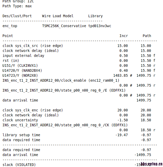

到代码里面查找有关路径终点的代码,发现rst连接到了ctrl_enc_reg的异步复位端,并且ctrl_enc_reg的输出带了七八个与INST_ADDR12_00同类型的模块input_enable端口(同步使能),推测这样的设计造成了扇出过高,现在尝试修改代码修正该问题。
但仍有疑问的是:
1. 综合脚本已经对顶层rst设置了dont_touch和ideal属性,为什么还会看到有关rst的路径上有如此大的时延;
2. 上述的设计我可以理解为异步复位同步释放的设计,但在综合时我应该如何对这样的端口进行约束?
现在综合后的timing结果如何,
因为rst还没做tree, 因此建议 set_ideal_network -no_prop [get_ports rst ]然后再报timing,
高delay 通常是hfn 造成的,
现在综合后的timing结果如何,
因为rst还没做tree, 因此建议 set_ideal_network -no_prop [get_ports rst ]然后再报timing,
高delay 通常是hfn 造成的,
对相关的内部节点设置了dont_touch和ideal属性,时序没有问题。在ICC中place_opt之后也满足setup约束(此时相应的约束)。单独对addr_ctrl_reg/QN 进行compile_clock_tree -high_fanout_nets极大地降低了时延,但是还有-5左右的slack。到这里感觉就是设计的问题,我一开始对几个pat_*端口设置false_path属性是不是有问题,这几个是模式选择端口,这几个端口应该如何设置?
可以不设,除非引起很大的input violation,input delay设成0就行了