各位兄弟 石墨烯晶片時代快到了
可否詳細介紹一下~
引述 UCSB Nanoelectronics Research Lab 之資料
Let's Make the Entire Chip from GrapheneBy Dexter JohnsonPosted 24 Oct 2013 | 19:27 GMT
- Share
- |
- Email
- |
- Print
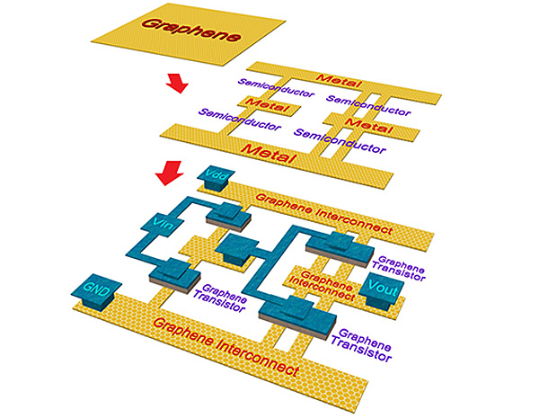
Illustration: UCSB Nanoelectronics Research Lab
The International Technology Roadmap for Semiconductors (ITRS) predicts that by 2015, copper-based vias that connect the silicon surface to a chips' wiring and connect one layer of wiring to another simply will not be able to do the job anymore. That day is a little over a year away—practically tomorrow in technological innovation terms. As a result, there is a bit of a scramble to find alternatives—not just for vias but for all sorts of interconnects used in integrated circuits (ICs).
Researchers at the University of California, Santa Barbara (UCSB) have taken an initial step in offering one possible alternative: “an integrated circuit design scheme in which transistors and interconnects are monolithically patterned seamlessly on a sheet of graphene.”
It’s been over 30 months since IBM demonstrated that it could make an integrated circuit using graphene; in this most recent research, the UCSB team demonstrated, using a computer model, that its design is feasible. So where is the disconnect (pun intended)?
The IBM work involved a graphene field-effect transistor and inductor and other circuit components that were monolithically integrated on a single silicon wafer. The UCSB design proposes that every bit of the IC be made from graphene.
"In addition to its atomically thin and pristine surfaces, graphene has a tunable band gap, which can be adjusted by lithographic sketching of patterns—narrow graphene ribbons can be made semiconducting while wider ribbons are metallic,” explained Kaustav Banerjee, professor of electrical and computer engineering and director of the Nanoelectronics Research Lab at UCSB, in a press release. “Hence, contiguous graphene ribbons can be envisioned from the same starting material to design both active and passive devices in a seamless fashion and lower interface/contact resistances."
In the paper that was published in the journal Applied Physics Letters(“Proposal for all-graphene monolithic logic circuits”) the researchers demonstrate “that devices and interconnects can be built using the 'same starting material'—graphene.” While that is intriguing, what may really garner the interest of the semiconductor industry is the research paper's claim that, “all-graphene circuits can surpass the static performances of the 22-[nanometer] complementary metal-oxide-semiconductor devices.”
Commenting on the research, Professor Philip Kim at Columbia University noted: "This work has demonstrated a solution for the serious contact resistance problem encountered in conventional semiconductor technology. [It presents the] innovative idea of using an all-graphene device-interconnect scheme. This will significantly simplify the IC fabrication process of graphene based nanoelectronic devices."
Illustration: UCSB Nanoelectronics Research Lab
歐洲正在用 1 billion 歐元 打造一個石墨烯谷 (美國有矽谷)
Thank you~
LZ有没有相关资料,或者你在三楼的内容出自哪里,给我一份,谢谢。lwjee_06@126.com
为什么不是忆阻器?
快?
十年以后吧。
理论与现实是有差距的。
2010諾貝爾物理獎就是用膠帶一直撕石墨可以做出很小片的石墨烯
兩年前我大學同學就在IBM高等研究中心開發出全世界第一個超大面積石墨烯量產製成與石墨烯電晶體 (上面文章寫的就是我同學在IBM做的). 現在各國都在做. 時代進步很快.
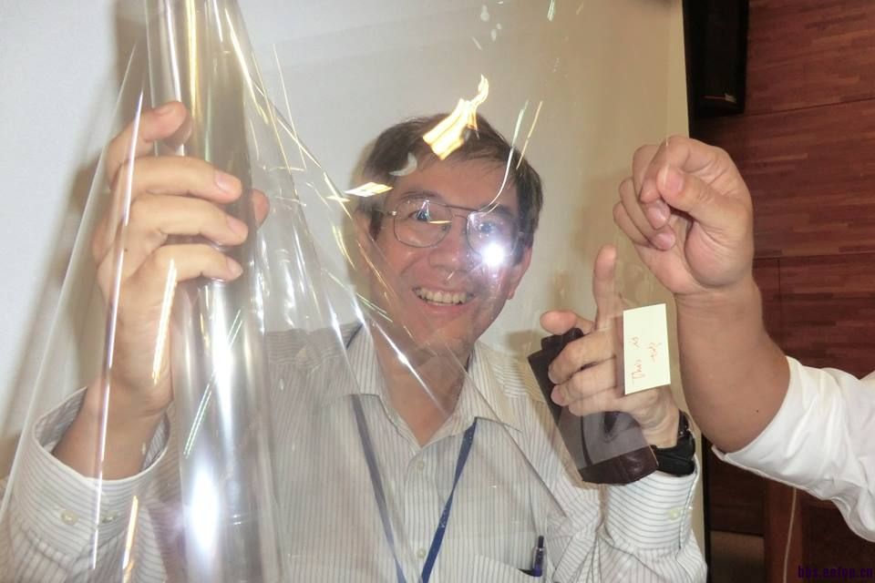
我同學 (Dr. Yu Ming Lin) 在一個展示會議上demo石磨烯的照片 照片中的人不是我同學 (日本東北大學單原子層研究群似乎對這很有興趣)
Dr. Yu Ming Lin, who was at MIT, IBM and is now in Bluestone Company, showed us CVD graphene on PET (PET bottle material)
on the occasion of a meeting in Taiwan in the last week.
They used so-called bubbling technique (H_2 bubble generation by electric current in H_2O) for detaching graphene
from Cu surface without chemical removal of Cu. The price of this
sample is 400 USD for A4 size. If you are interested in this,
contact to Bluestone. (You can find YOUTUBE by "bluestone, graphene").

各位如果有興趣可以欣賞一下我同學的事蹟
http://www.gr-sci.net/FinFET 从发明到实际应用还用了10几年的时间,石墨烯要在集成电路中应用要解决的问题还很多,最大的问题是材料的制备。成本越来越成为新技术推广的障碍。
這些都是高度資本技術密集企業做的 可能最後都要靠國家力量來突破