ST EVALSP1340CPU嵌入600MHz MPU开发方案
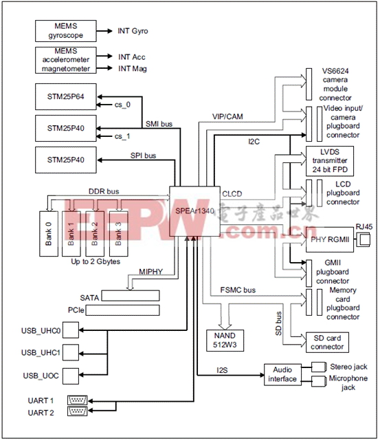
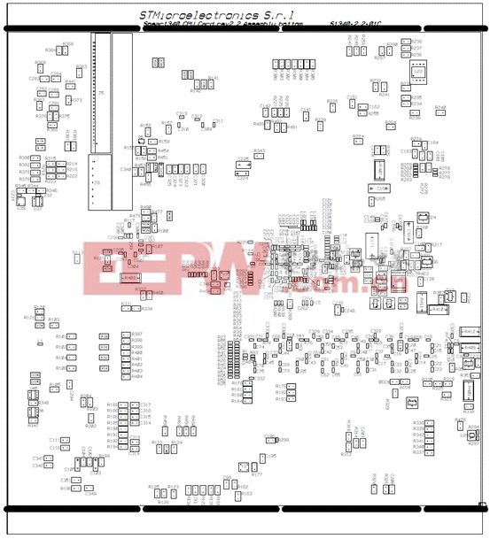
– Debug and trace interfaces: JTAG/PTM 图1.SPEAr1340架构框图 EVALSP1340CPU评估板 This evaluation board is intended to be used to: ● enable quick evaluate and debugging of software for the SPEAr1340 embedded MPU ● act as a learning tool for rapid familiarity with the features of the SPEAr1340 ● provide a reference design to use as a starting point for the development of a final application board The EVALSP1340CPU board is equipped with interfaces to the high-speed peripherals embedded in SPEAr1340 device. 图2.EVALSP1340CPU评估板外形图 EVALSP1340CPU评估板主要特性: ● SPEAr1340 embedded MPU ● 4 DDR3 chips (32-bit) 1 GB ● Serial NOR Flash, 8 MB ● 8-bit NAND Flash, 2 Gb ● 16-bit NAND Flash expansion connector ● Audio stereo jack and microphone ● Two USB 2.0 high speed host ports ● One OTG 2.0 high speed port (Micro USB-AB) ● One 10/100/1000 Ethernet port ● One PCIe X1 Root Complex connector ● One SATA connector ● One SDIO connector ● One UART serial port (up to 115 Kbaud) ● LCD connectors (LVDS bus - TFT panel) ● Camera module ● MEMS (accelerometer magnetometer) ● Debug port (CPU JTAG connector) Optional ● 10 LCD kit - order code EVALSP1340LCD ● CLCD Video HDMI transmitter plugboard - order code EVALSP1340HDM 图3.EVALSP1340CPU评估板方框图 图4.EVALSP1340CPU评估板电路图(1) 图5.EVALSP1340CPU评估板电路图(2) 图6.EVALSP1340CPU评估板电路图(3) 图7.EVALSP1340CPU评估板电路图(4) 图8.EVALSP1340CPU评估板电路图(5) 图9.EVALSP1340CPU评估板电路图(6) 图10.EVALSP1340CPU评估板电路图(7) 图11.EVALSP1340CPU评估板电路图(8) 图12.EVALSP1340CPU评估板电路图(9) 图13.EVALSP1340CPU评估板电路图(10) 图14.EVALSP1340CPU评估板电路图(11) 图15.EVALSP1340CPU评估板电路图(12) 图16.EVALSP1340CPU评估板电路图(13) 图17.EVALSP1340CPU评估板电路图(14) 图18.EVALSP1340CPU评估板电路图(15) 图19.EVALSP1340CPU评估板电路图(16) 图20.EVALSP1340CPU评估板电路图(17) EVALSP1340CPU评估板材料清单: 图21.EVALSP1340CPU评估板元件布局图(1) 图22.EVALSP1340CPU评估板元件布局图(2) 图23.EVALSP1340CPU评估板元件布局图(3)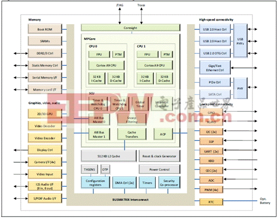


开发 方案 MPU 600MHz EVALSP1340CPU 嵌入 ST 相关文章:
- 嵌入式软件设计中查找缺陷的几个技巧(03-06)
- 基于算法的DSP硬件结构分析(04-02)
- Windows CE下驱动程序开发基础(04-10)
- DSP+FPGA在高速高精运动控制器中的应用(05-17)
- 基于USB接口和DSP的飞机防滑刹车测试系统设计(05-19)
- 一种基于DSP平台的快速H.264编码算法的设计(05-19)