Design Challenges for an Ultra
Introduction
This is a reference design for a low-jitter clock source for high-speed data converters. The goal is to achieve
Design Requirements
The maximum intended frequency for this clock design is 2GHz. However, there are alternate VCOs (voltage-controlled oscillators) and prescalers available that can extend the frequency higher, each device producing differing results. This reference design, simulation tests, and results are focused on performance only at 2GHz output frequency.
Some high-speed converters use both edges of the clock signal for internal timing. Consequently, a critical design requirement is a 50% duty cycle. Additionally, the targeted output drive is 10dBm into 50Ω, or a 2VP-P differential.
Basic Synthesizer Design

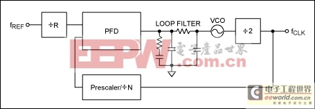
Figure 1. Traditional PLL.
The simplest solution is a traditional PLL circuit, shown in Figure 1. As stated above, a 50% duty cycle is critical. Consequently, the VCO is run at twice the desired clock rate (4GHz), and a divide-by-2 provides the desired output frequency and duty cycle. The divider adds jitter and is, therefore, placed within the PLL loop to take advantage of noise shaping.
The loop filter is lowpass for reference noise and highpass for VCO noise. It also determines the loop's settling time. Since this is a fixed-frequency application the loop settling is not an issue; the filter bandwidth can be optimized for noise only. A low-bandwidth filter makes reference noise easier to manage, but puts the noise burden on the VCO. A wide-bandwidth filter would do the opposite.
Research of available VCOs and reference oscillators reveals that the "best of both worlds" can be obtained, although this goal will still necessitate a balancing act between the two components. An ultra-low-noise VCO and reference oscillator are needed for this design. To determine just how low the noise must be, the phase-noise requirements for a 100fs jitter specification need to be determined.
Phase noise is specified as a level relative to the carrier, and versus the offset frequency (dBc/Hz). All phase noise integrated together becomes the phase-noise power, which can be compared to the fundamental power. This phase noise is divided by the fundamental frequency to obtain jitter.
For example, suppose that a 2GHz VCO has a SSB (single-side-band) phase noise of -110dBc/Hz from 10kHz to 100kHz. The bandwidth of interest is 90kHz, resulting in 49.5dB. Consequently, the integrated noise is -60.5dBc. The SSB noise power is:
So the RMS noise voltage is:
The factor of 2 inside the square root ensures that both sidebands1 are included.
Jitter is calculated by:
Equation 3 only gives the jitter contribution for the 10kHz-to-100kHz offset. Other offsets must be included to determine the overall jitter.
There is an alternative approach. We can also work backwards, go from jitter to phase noise. Consequently, for a desired 100fs of jitter at 2GHz:
SSB relative noise power is:
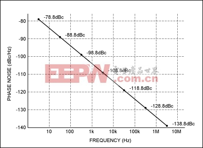
The result from Equation 5 equals -61dBc of total integrated (SSB) noise power. Assuming that phase noise is equally distributed from 1Hz to 10MHz, then the conversion to dBc/Hz produces the following phase-noise mask (Figure 2).
Figure 2. Phase-noise mask.
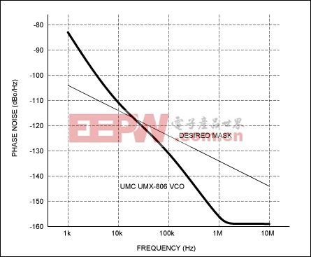
There is no question that 100fs of jitter at 2GHz is an aggressive phase-noise specification, especially in the 10kHz to 100kHz range. At 10kHz the required phase noise is about -114dBc/Hz, which few discrete2 VCOs can achieve, and certainly none that are integrated. Universal Microwave Corporation (UMC) makes VCOs which meet this level of purity. The UMX-series is produced in a range of 500MHz to 5GHz with 10kHz phase-noise specifications that often exceed -112dBc/Hz typical. Even the UMX VCOs' worst-case specification meets our requirements.
Figure 3. UMX-806-D16 phase noise with the desired phase-noise mask indicated.
Figure 3 shows the worst-case phase noise for a 4GHz VCO (UMX-806-D16) and our desired phase-noise mask. Below 20kHz the phase noise for this VCO is too high, but the PLL loop filter bandwidth can be designed to suppress low-offset VCO noise. Above 10kHz phase noise is no problem, assuming that nothing else degrades it. Recall that the phase-noise requirements were derived for a 2GHz oscillator. Figure 3, however, shows the curve for a 4GHz oscillator, which is needed because of the additional divide-by-2 used to guarantee a 50% duty cycle. The divide-by-2 reduces the VCO phase noise by 6dB, so the entire curve will shift down by that amount, assuming that the divider itself does not degrade the overall phase noise.
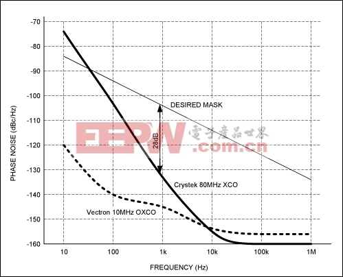
Note that the reference oscillator will contribute noise, but mostly at offsets lower than the loop filter bandwidth. Figure 4 shows a plot of a Crystek? 80MHz crystal-controlled oscillator and the desired phase-noise mask. It is important to remember that the PLL frequency gain multiplies the reference phase noise. Therefore, for an 80MHz crystal and a 2GHz output, the gain is 25. Consequently, the Crystek curve should be shifted up by 28dB. This adjustment, however, means that the reference phase noise will be too high below about 1kHz.3 However, the phase-noise mask assumes that the integrated noise power is equally distributed across the offset spectrum. It does not have to be, of course, so stellar phase noise beyond 1kHz added to the excessive sub-1kHz noise can still give an overall integrated phase noise that meets our jitter spec.
Figure 4. Reference phase noise.
Nevertheless, the phase-noise analysis in Figure 4 also includes an oven-controlled oscillator (OCXO) from Vectron, which has significantly less phase noise. Note that OCXOs have the tendency to burn excessive amounts of power (specified in Watts).
模拟电路 模拟芯片 德州仪器 放大器 ADI 模拟电子 相关文章:
- 12位串行A/D转换器MAX187的应用(10-06)
- AGC中频放大器设计(下)(10-07)
- 低功耗、3V工作电压、精度0.05% 的A/D变换器(10-09)
- PIC16C5X单片机睡眠状态的键唤醒方法(11-16)
- 用简化方法对高可用性系统中的电源进行数字化管理(10-02)
- 利用GM6801实现智能快速充电器设计(11-20)
