ESD保护I/O端口
时间:03-24
来源:本站整理
点击:
Abstract: This applicaTIon note describes how ESD threatens electronic systems, type of damage inflicted, how ESD is generated, test methods and waveforms used, human body and machine models for tesTIng, IEC compliance levels, contact and air discharge. ProtecTIon methods are described and Maxim's approach to ESD protecTIon is detailed. Guidelines are given for selecting ICs with high resistance to ESD. RS-232 I/O ports are specifically considered.
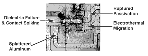
Electrostatic discharge (ESD) can threaten an electronic system when someone replaces a cable or even touches an I/O port. Discharges that accompany these routine events can disable the port by destroying one or more of its interface ICs (Figure 1). Such failures can also be costly—they raise the cost of warranty repairs while diminishing the product's perceived quality.

Figure 1. ICs with inadequate ESD protection are subject to catastrophic failure—including ruptured passivation, electrothermal migration, splattered aluminum, contact spiking, and dielectric failure.
ESD has another way of causing trouble. Manufacturers may soon be barred from selling to the European community unless their equipment meets minimum levels of ESD performance. These two factors, coupled with the increasing amount of electrical communication between computers and computer-related equipment, lend emphasis to the need for engineers to understand ESD.
A proper understanding of ESD requires an awareness not only of the voltage levels involved, but also of the voltage and current waveforms, IC-protection structures, test methods, and application circuits. These matters are discussed in the following sections.
The triboelectric series (Table 1) describes this charge affinity between various materials. Charge transfer occurs when any two items on the list are brought into contact. Materials higher in the series acquire positive charge, and those lower in the series acquire negative charge.1 The net charge and resulting electrostatic voltage is greater for items farther apart on the list.
Table 1. Triboelectric Series

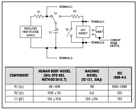
The applied signal in this test is a current waveform derived from a circuit called the human body model (Figure 2), which simulates the capacitance and source impedance typical of a human body. (Circuit layout is critical, because the actual waveform delivered at the IC depends also on parasitic inductance and capacitance associated with the test connections and pc board.) The resulting current waveform represents the ESD that occurs when a person touches an object, such as an IC.

Figure 2. Substituting different component values as shown yields discharge circuits known as the human body model, the machine model, and the IEC 1000-4-2 model (human holding a metallic object).
The other method, which differs from the above only in the values for R and C, was developed by the Electronic Industries Association of Japan (EIAJ). Called IC-121 and based on a circuit called the machine model (Figure 2), it applies a current waveform similar to that produced when an IC makes contact with its handling machinery. By mimicking the ESD events caused by charges that accumulate on moving parts, the waveform simulates static discharges seen during machine assembly.
The two methods are complementary, so you shouldn't choose one over the other. Because ESD can affect ICs during manufacturing, during pc board assembly, and after the end product is put into service, a test based on the human body model and the machine model together provides adequate assurance regarding the IC's tolerance for the rigors of manufacturing and insertion.
Some ICs, whose pins are exposed to the outside world through connectors, can encounter ESD even when mounted on a pc board within an enclosure. ESD exposure is less likely for the other pins, which are connected to circuitry on the board. For this class of IC, a test method such as Method 3015.7 (which tests pin combinations) does not provide an adequate representation of ESD susceptibility for the input/output (I/O) pins.
Electrostatic discharge (ESD) can threaten an electronic system when someone replaces a cable or even touches an I/O port. Discharges that accompany these routine events can disable the port by destroying one or more of its interface ICs (Figure 1). Such failures can also be costly—they raise the cost of warranty repairs while diminishing the product's perceived quality.

Figure 1. ICs with inadequate ESD protection are subject to catastrophic failure—including ruptured passivation, electrothermal migration, splattered aluminum, contact spiking, and dielectric failure.
ESD has another way of causing trouble. Manufacturers may soon be barred from selling to the European community unless their equipment meets minimum levels of ESD performance. These two factors, coupled with the increasing amount of electrical communication between computers and computer-related equipment, lend emphasis to the need for engineers to understand ESD.
A proper understanding of ESD requires an awareness not only of the voltage levels involved, but also of the voltage and current waveforms, IC-protection structures, test methods, and application circuits. These matters are discussed in the following sections.
ESD Generation
Electrostatic charge appears when two dissimilar materials come together, transfer charge, and move apart, producing a voltage between them. Walking on a rug with leather soles, for example, can generate voltages as high as 25kV. The level of electrostatic voltage induced depends on the relative charge affinity between rug and shoe leather, the humidity, and other factors.The triboelectric series (Table 1) describes this charge affinity between various materials. Charge transfer occurs when any two items on the list are brought into contact. Materials higher in the series acquire positive charge, and those lower in the series acquire negative charge.1 The net charge and resulting electrostatic voltage is greater for items farther apart on the list.
Table 1. Triboelectric Series

ESD Test Methods
Two methods are commonly used for testing the ESD susceptibility of integrated circuits. The oldest, MIL-STD-883 Method 3015.7, was developed as an aid in understanding the precautions necessary for packaging and handling ICs. This method tests each package pin against other groups of pins, and classifies the device according to the lowest voltage for which failure occurs.The applied signal in this test is a current waveform derived from a circuit called the human body model (Figure 2), which simulates the capacitance and source impedance typical of a human body. (Circuit layout is critical, because the actual waveform delivered at the IC depends also on parasitic inductance and capacitance associated with the test connections and pc board.) The resulting current waveform represents the ESD that occurs when a person touches an object, such as an IC.

Figure 2. Substituting different component values as shown yields discharge circuits known as the human body model, the machine model, and the IEC 1000-4-2 model (human holding a metallic object).
The other method, which differs from the above only in the values for R and C, was developed by the Electronic Industries Association of Japan (EIAJ). Called IC-121 and based on a circuit called the machine model (Figure 2), it applies a current waveform similar to that produced when an IC makes contact with its handling machinery. By mimicking the ESD events caused by charges that accumulate on moving parts, the waveform simulates static discharges seen during machine assembly.
The two methods are complementary, so you shouldn't choose one over the other. Because ESD can affect ICs during manufacturing, during pc board assembly, and after the end product is put into service, a test based on the human body model and the machine model together provides adequate assurance regarding the IC's tolerance for the rigors of manufacturing and insertion.
Some ICs, whose pins are exposed to the outside world through connectors, can encounter ESD even when mounted on a pc board within an enclosure. ESD exposure is less likely for the other pins, which are connected to circuitry on the board. For this class of IC, a test method such as Method 3015.7 (which tests pin combinations) does not provide an adequate representation of ESD susceptibility for the input/output (I/O) pins.
- LinkSwitch的电磁兼容性设计(07-10)
- EMI防治技巧与挑战(03-19)
- 用最佳终端匹配策略降低电磁辐射的干扰(02-11)
- 电磁干扰(EMI)抑制技术(03-10)
- 汽车元件的EMI抗扰性测试(04-02)
- 通过PCB分层堆叠设计控制EMI辐射(04-02)
