ESD保护I/O端口
时间:03-24
来源:本站整理
点击:
- Excessive local heating
- Melted silicon
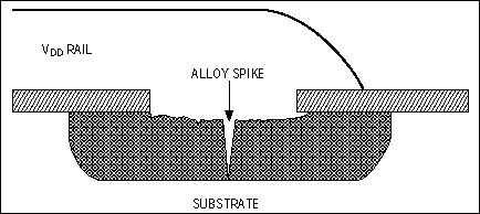
- Spiked junctions, caused by a short that dissolves aluminum in the silicon (Figure 5)
- Damaged metal lines
- Gate-oxide failure due to excessive voltage
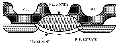
- Transistor damage due to electrothermal migration (Figure 6)

Figure 5. High-ESD current in an IC can "spike" a junction by partially dissolving the aluminum contact in silicon, causing a permanent short to the layer below.
Figure 6. Electrothermal migration (ETM) in an IC can set the stage for damage in the presence of an ESD event. The resulting high current and high voltage can cause a short circuit or low-impedance path between the terminals of a transistor.Protection Methods
To protect against ESD, a designer can either add the protection externally or choose ICs with high levels of protection built in. Protection circuitry includes metal-oxide varistors and silicon avalanche suppressors such as the TransZorb. These devices are effective but expensive (silicon avalanche protectors cost as much as $0.30 per line). External ESD protection also consumes valuable board area and adds capacitance to the I/O line.
To overcome these limitations, manufacturers have repeatedly raised the level of ESD protection in their ICs. Maxim, for example, now provides ±15kV protection for RS-232 ICs, whether tested in accordance with IEC 1000-4-2 or the human body model.Maxim's Approach to ESD Protection
An ESD current waveform is characterized by extremely fast rise times, so its progress through an IC is strongly affected by the circuit's distributed parasitic impedances. Therefore, attention to the external layout will ensure maximum performance by the IC's internal protection networks. Maxim recommends the following practice with respect to its interface ICs:- Follow standard analog-layout techniques, placing all bypass and charge-pump capacitors as close to the IC as possible.
- Include a ground plane on the pc board.
- Minimize trace inductance and capacitance.
- Place the IC as close to the I/O port as possible.
Because the intent of these tests is to assess the ESD performance of an IC installed in end equipment, the test setup should cause ESD currents to flow along the same paths as they would in that equipment. Zaps should be administered with respect to the IC's ground pin. (As stated in IEC 1000-4-2, circuit ground usually connects to the equipment chassis.) Maxim recommends the model NSG 435 ESD gun by Schaffner Instruments (Switzerland) for the IEC 1000-4-2 method, and the model 4000 ESD tester by IMCS (a division of Oryx Technology Corporation, Fremont, CA) for the modified 3015.7 method.
You should check for failures by monitoring three parameters after each zap. First, the supply current should remain constant (an increase may indicate latchup or internal damage). Second, the transmitter output voltage should continue to meet the ±5V minimum levels for RS-232 transmission. Third, the receiver input resistance should remain between 3kΩ and 7kΩ (ideally, it should remain at a constant level in that range). Be sure to zap and test the device in all its modes: normal operation, shutdown, power off, transmitter high/low, etc.
Guidelines for Selecting ICs with High Resistance to ESD
Here are some questions to resolve before choosing an IC (particularly an RS-232 transceiver) that must withstand high levels of ESD:
- LinkSwitch的电磁兼容性设计(07-10)
- EMI防治技巧与挑战(03-19)
- 用最佳终端匹配策略降低电磁辐射的干扰(02-11)
- 电磁干扰(EMI)抑制技术(03-10)
- 汽车元件的EMI抗扰性测试(04-02)
- 通过PCB分层堆叠设计控制EMI辐射(04-02)
