zero if dc offset
I think this will be controlled not solve,but how?
someone tell me that there are some digital calibration technique to control the bias?but this maybe too complicated a technique.
can anyone offer some details of the dc offset calibration technique in the picture.
(ac coupling or feedback integrator/dc servo-loop or other....)
thankS, and again thank you.
generally the dc offset is cancelled in baseband side through dsp.
then as RF designer,how to controll or minimize the problem resulted from the dc offset, even some simple feedback from the vga/pga ?
i think a high pass filter might be helpful to minimize the dc offset,but it is eventually solved in baseband side.
Added after 2 minutes:
note the high pass filter might slow down the data rate,and it must be a fir type whose phase-response is linear.
it is right,the final and main part of the calibration should be in the dsp baseband.
but as a front-end designer besides some layout technique to improve the lo feedthrough or other,
I think there would be other things you have to do,at least a feedback loop to prevent the dc offset be amplified by a 70db gain vga chain and saturate the latter stages
what I am intereted in is how the feedback loop is realized ,is it some simple cmfb technique used in opamp or even some very complicated matter involved some dacs or analog filters.....
again thanks for your reply
well,i think this must be technical secret for RFIC vendors,maybe no one can point out which way you should go.just try it.
good luck to you.
Hi,
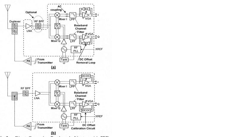
At this time several techniques are used to provide dc offset cancellation.
On the first picture simple servo-loop is used to remove dc offset. Servo-loop likes high pass filter with cut off frequency about several kHz. So, received signal is damaged near dc. Usually this technique is used in CDMA or OFDM (mobile TV, WLAN...) receivers. Because in this case it is possible to recover signal.
In GSM receiver second technique is used (second picture). Before receiving the next burst autocalibration of DCOC is provided: feeddback integrator is activated, bias voltage is set to cancel dc offset and then this bias is keept. This set is true only for receiving the burst. Before receiving ...
Rgds