help S-parameter test problem
It's difficult for me understanding Your problem, I try a generic answer.
As You know, the s par completely describe the behaviour of the respective network (the FET for instance).
Regardless to what is connected outside the reference planes of the network ports.
So, if You have the measured spar of the FET (the FET alone - common source), You may put it on both virtual circuit (ADS) or real circuit and perform measurement.
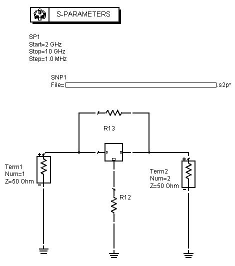
A different scenario (the reverse engineering) . In real case, if You, helped by a VNA, may measure spar of Your circuit and Your target is get FET spar, You may put the measured spar of the circuit into a simulator, and add:
a resistor of value -R12 over GND line
a resistor of value -R13 between In and Out.
and perform the simulation, the result is spar of the FET
I Hope This help You
parameter 相关文章:
- S parameter extraction for MOSFET internal parameters
- Parameters S12 Reverse transmission coefficient
- Can you help me get S-parameter file of Mitsubishi MGF4937AM and Infineon CFY67
- MIMO Parameters: TARC, CCL, MEG
- s Parameters of LNA Improvement
- S-Parameters De-embedding using matlab/frequency vector problems