Design of transistor test fixture
I am designing my own Test Fixture to measure a packaged transistor, the TF is composed of 2 launches (with biasing path) and a line to make the TRL calibration.
The TF center frequency is 2185MHz and it's 50 ohms reference impedance. I would like to be able to perform measurement from 0.5GHZ to 8GHz, but It seems that the launch has S21 resonnant frequency about 4.5 GHz, it is a problem.

This is due to bias circuit. i don"t know how to get a flat S21 full bandwidth.
My project is available here.
I don't have ADS, so I cannot open the project, but from the image, it seems that the biasing path is acting like a stub. Try to remove it and simulate.
You need to design a wideband biasing or use an external bias tee.
I hope it can help.
Mazz
Mazz,
Tha biasing path is composed of a lambda/4 ustrip line combined with a shunt capacitor under Taconic RF35 substrate.
You say me that I should use an inductor like that ?
but with this kind of inductor, the limit of current is about 1A (CW), it is too low for my application
With microstrip line it"s more easy to reach high level of current (3 or 4 A in my case).
I havent designed any large bandwidth tee bias, but...
Those inductors are for very large bandwidth (>10 GHz, if I well remember.)
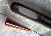
Some time ago I opened up and repaired a bias tee: they used a circuit made by different sized inductors (there was also a transformer) to prevent self resonant freq (see http://www.qsl.net/n9zia/wireless/pics/bias_tee.png to have an idea).
Or you can try using large bandwith stubs + some discrete.
I hope it can help.
Mazz
Design transistor fixture 相关文章: