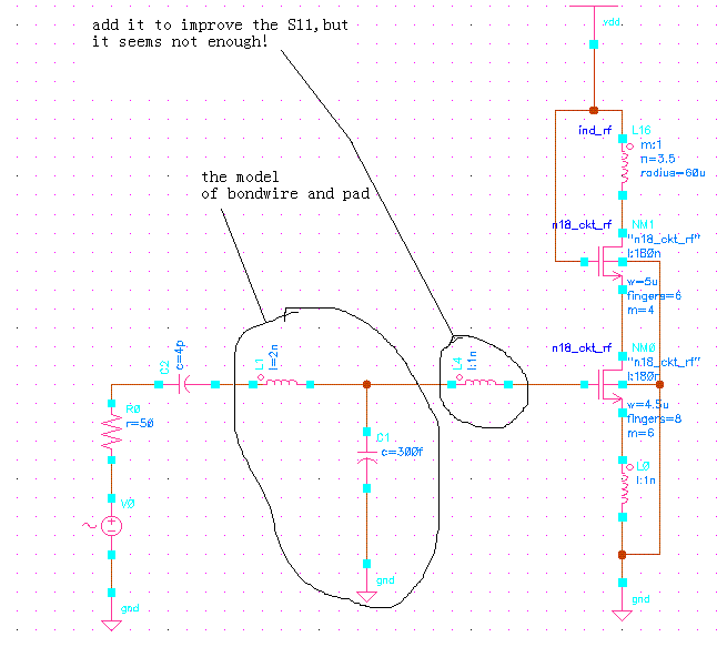
Input match of a CS-LNA considering the bondwire and pad
input match network.Considering the effect of bondwire and pad of input signal,the quetion seems more difficult to me,the schematic is as follows ,how can I make an input match network to achieve both a good S11 and NF at the same time ,thank you!
ps: the book " microwave egineer" is usefull for RF designing?
the source degenration inductor used to increasee the real part of the input impedance , while the gate inductor used to eleimtae the imaginary capacitive part , but u have another section u need to know how this section affect the input imedance of ur circuit , then re design the Ls and Lg to give u the best result
sure if u read about matching circuits in microwave books will be very usefull
khouly
thank u very much for ur advise ,i think i should learn more theory about matching firstly,
any how it becomes more complicated consideing the effect of bondwire and pad of input, output,gnd and vdd,and my circuit is working on 3-5GHz, it's really awful things!
sure the multi Ghz RFIC , these effects of bondwires and pads must be taken into account ,
u need to check how the bondwire intuctance will affect the impedance
khouly
May i know what are the books for matching network concept...Please kindly tell me...
- CST script - command do not get registered in the history
- CST accuracy control beyond the mesh density
- CST SAR problem at 90% for breast cancer detection
- [CST-MWS] How to get data-points for 2D geometry?
- drawing meander line helix in CST
- [Basics] Why is (RF) current "flowing back" underneath the "forward line" ?