Could someone help on this VDD bypass circuit?
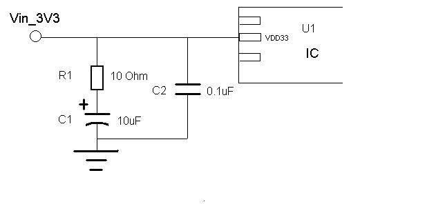
The reason of resistor is to increase the R1*C1 time constant, lowering in this way the decoupling frequency of the circuit.
Generally this approach is used in LNA design for improving IP3, and in Power Amplifier design to prevent low frequency oscillations.
Thanks. I can not fully understand.The circuit is used for an RF receiver below 900MHz. I can understand that the R1 decreases the circuit's frequency and improves the noise of the node between R1 and C1. But what about the Vin_3V3 node?
---------- Post added at 09:21 ---------- Previous post was at 09:16 ----------
Google "bypass capacitor" and find an intersil appnote http://www.intersil.com/data/an/an1325.pdf (figure 22). A similar circuit is used without a detailed explain.
I've seen it in audio amplifiers psu, i think it resembles a zobel filter but for the power supply and i have seen it make a difference in an ic amplifier (lm3886)
Speaker Zobel / Impedance Equalization Network Circuit Calculator
Alex
In the zobel filter, the capacitor was used to cancel the inductance of the speaker.The resistor can broad the bandwidth. In my case, it will make sense if the VDD node's original impedance is inductive. But does a normal LDO or power supply output is inductive?
The circuit i was talking about (amplifier) didn't a have regulator, it was only a full wave bridge for symmetric supply,
i believe that the "zobel" circuit helped with the inductance of the electrolytic capacitor (4700uf) if the high frequency.
I don't know about the LDO.
Alex
---------- Post added at 03:26 ---------- Previous post was at 03:19 ----------
There is also an article http://www.bcae1.com/switchingpowers...nfoslva115.pdf
Maybe the resistor has something to do with the ESR of the capacitor...
Alex
Thanks. It is meaningful. So the capacitor for the LDO load should has a ESR range.It will not work if too high or too low.
Can you explain this technique in detail ?
Here is a detail explain on VDD bypass(Not about IIP3 ). http://www.designers-guide.org/Design/bypassing.pdf
- In PA, if the bias is VDD then how can swing be 2*VDD with inductive load
- Switching Vdd of LNA (SKY67151-396LF)
- When to connect RF Bypass capacitor, and a Resistor in place of RF choke?
- Method for bypassing LNA
- RF preamplifier bypass using spdt switch
- Why all RF designs bypass capacitors are much larger than blocking capacitor?