Frequency phase comparator in PLL HCT4046
a) reference input: 370KHz, phase=0 (square wave) , comparator input: 370KHz, phase=0 (square wave), comp output: 4.8Vdc
b) reference input: 370KHz, phase=0 (square wave) , comparator input: 310KHz, phase=0 (square wave), comp output: 4.86Vdc
c) reference input: 370KHz, phase=0 (square wave) , comparator input: 370KHz, phase=60 (square wave), comp output: 4.76Vdc
d) reference input: 370KHz, phase=0 (square wave) , comparator input: 330KHz, phase=60 (square wave), comp output: 4.69Vdc
i use Vcc=5V and GND for the HCT4046. The result i obtain seem like very weird. It keep remain in 4.6V-5V and seem like no comparison between frequency and phase.
btw, if my Vcc=5V, is it mean that the input signal should have amplitude of 5V?
I have not much knowledge in PLL especially related to frequency phase comparator. please give some advice to me. thank a lot.
My guess is the PLL isn't locked so I think your nominal frequency is set incorrectly. When it is locked then you will get some sensible results.
Keith.
is it the lock range is between VCO output minimum frequency and maximum frequency? according to the data sheet, the control range of input voltage for VCO is 1V< VCOinput< 0.9Vcc. So, i apply the following voltage to VCO and obtain the following result:
a) VCOin = 1V, VCOout = 103.1KHz
b) VCOin = 2.5V, VCOout = 230.7KHz
c) VCOin = 4.5V (0.9Vcc), VC0out = 433.5KHz
so the lock range is between 103.1KHz and 433.5KHz, if my reference fequency = 370KHz, is it ok? btw, thx for reply... need help desperately
I think I misunderstood your original setup, although I think you are misunderstanding the phase comparator! Depending on which phase comparator output you are looking at, the phase comparator gives a signal which relates to the phase difference between the signals but it is a rectangular wave and the average voltage will vary from 0V to 5V depending on the phase for PC1. PC2 is different. Here is a simulation of the 4046 PC2 as it tries to lock.
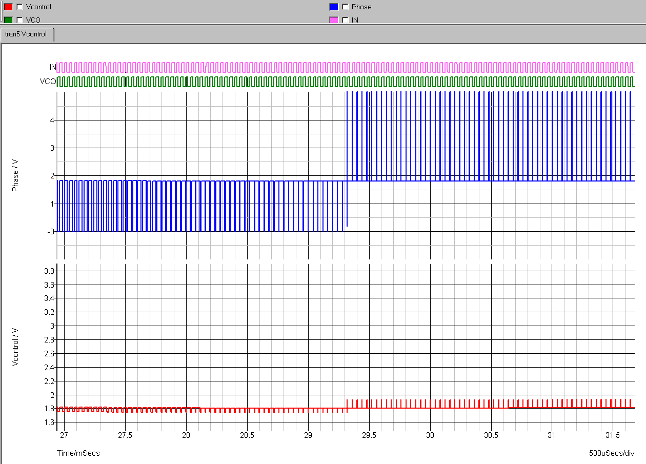
If you look at the phase plot in blue you will see it goes through a period of negative pulses followed by a period of positive ones as it tries to lock. Eventually it settles down "floating". However, if you try to probe it then you will most likely load it and not see a correct value. Which phase comparator are you using?
Keith.
I am using Phase Comparator 2. So, do u mean that the output for PC2 is only 2, which is 0 and 1 ?
I think i really misunderstood the use of PC2. Can you give me some advice in how to test the PC2 ?
What do u mean by "if you try to probe it then you will most likely load it and not see a correct value" ?
Thank you very much.
Sorry, I don't understand that.
PC2 is an open drain output with NMOS & PMOS drivers. When the PLL is locked neither transistor will be driving so the pin will be floating. When the phase leads or lags then either the NMOS or PMOS will turn on for an amount of time depending on the phase shift. So ANY load will affect it.
Keith.
---------- Post added at 10:38 ---------- Previous post was at 10:37 ----------
You could probe it by using a CMOS opamp to buffer it.
Keith.