Sonnet EM Ports and Grounding
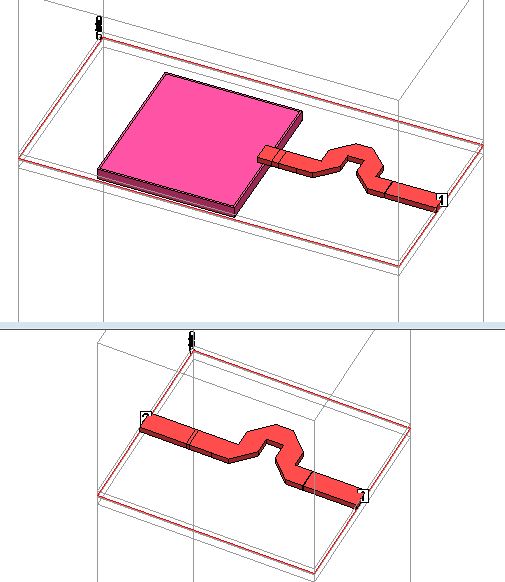
I am trying to simulate some inductors from 20 - 40 GHz using Sonnet software for my filter. Inductance value I am interested is 38 pH. Attached file contains the diagram of my inductor.
First I used standard box wall ports to obtain an inductance of 38 pH. The s2p file obtained from this simulation is used to simulate my filter circuit. In my filter circuit one port of this inductor is attached to the ground. I connected the second port of the s2p file to ground and it works fine.
Next I simulated the same inductor with the second port connected Sonnet ground. However, when I used this s1p file in my filter I get wrong results.
I compared the S11 of the both sNp files and they different even at low frequencies.
I also noticed that when I used co-calibrated ports to calculate the inductance the value of the inductance is different from the value simulated using sonnet box wall ports.
Can somebody help regarding these issues?
Thanks alot!
Hello Radike,
your 2-port and 1-port model have a different stackup. In the 2-port model, you have the thick silicon substrate below the inductor. In the 1-port model, you have deleted the silicon and now have lossless metal very close below the inductor. This does change the inductance a lot.
For cocal ports, you might see different results because the path of current is indeed different (going down through the silicon substrate instead of going to the side). This changes the fields and the inductance.
Best regards
Volker
Hi Volker,
Thank you very much for the reply. I have attached a wrong sonnet file. Sorry about that. I actually simulated with silicon but still I get different results. I am using Ideal vias and grounding.
Is it possible to know which ports give the most accurate results? Using box-wall or using co-cal ports?
I also noticed that every time when I increase the box size it affects my inductance value. Is it possible to know how to determine the appropriate box size?
Thank a lot!
Hi Radike!
We expect different results. Your lossless via is connected to the surface of the substrate and not to the global ground (Sonnet box). Now the current path in the lossy silicon substrate is part of your results.
Both are accurate, but describe diffent path of current. The question is which current path is more realistic for your circuit. You can see the current path (ground return) when you do View > View Subsections, open the 3D view and enable the "GLG metal".
In your two-port model, the return current can flow through the silicon and through the Sonnet box. If the box side walls are the "easiest" path for the current, it will take that path. Now the size of the box (distance to the side walls) will change the total results because the return path (here: through the box side walls) changes.
Now, what is the inductance of the line only without the box effect? This is the wrong question, because the inductance depends on the return path also (need closed loop!). Just model in the most realistic way, and include your return path in the EM model. If the return path is through the silicon and you have a one-port, that is the correct (best) model.
Best regards
Volker
Hi Volker,
Thanks a lot for the information!
Best Regards,
Radike
Hi Volker,
I am trying to simulate my circuit with the M1 layer as grounding. In the actual design this is connected through the ground pad using vias. In the sonnet simulation one side of my ground pad is connected to the sonnet box. And I have drawn the big metal layer in the lowest M1 layer. Is it possible to know in-order to simulate the real situation should my M1 metal layer touch the box walls. I simulated the two situation and there is a big difference between them.
The loss is more when the m1 layer touches the box wall.
Thanks a lot!
Radike
Hello Radike,
if your hardware connects to the substrate, you should do the same in the EM model. Connecting directly to the Sonnet box (=global ground for the ports) will create a different path for return current.
To connect vias to the substrate in the EM model, you can draw a metal polygon at the bottom side of the via. This increases the area where your via touches the conducting substrate. If you do not draw that metal polygon, the substrate contact will be only 1 cell wide along the edges of the hollow via.
Hi Volker,
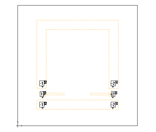
Thanks for the reply. I will be using on wafer probe testing. My reference grounding will be the two ground pins of the GSG pads. In this case should I include ports for the pads with -1 and -2 and simulate? I will be drawing a metal ground polygon which will be connected to the ground pads.
Thanks a lot!
Radike
Hello Radike,
attached is a simple example how I model GSG probes.
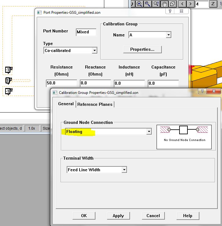
I use CoCal ports -1/+1/-1 group A and -2/+2/-2 group B, both with floating (local) ground reference.
Best regards
Volker
Hi Volker,
Thank you very much for the attachments. I have another 2 more questions.
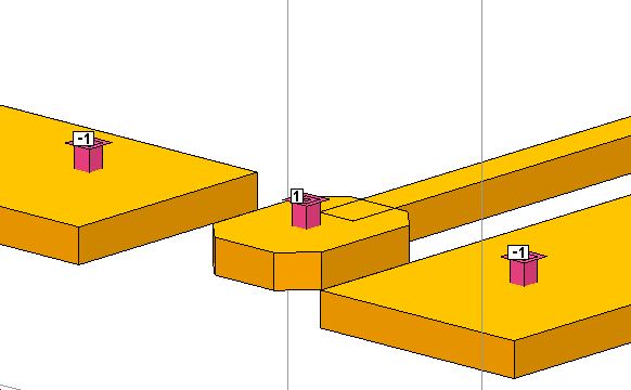
When defining the ports, did you first draw a small polygon and then another rectangle on top of it and attached a co-calibrated port at the edge of the rectangle or did you draw a via polygon and then attached the cocal port at the edge of the rectangle?
Also I would like to know if we have attached a box wall port at one side of the sonnet box whether Sonnet still considers this side of the box wall as ground reference.
Thanks a lot!
Best Regards,
Radike
These are two objects: via and metal rectangle. There is a small via that connects to the metal rectangle. The CoCal ports are on the edge of the metal rectangle.
I tried to upload the model, but the attachment function did not work.
The ground reference of the box wall ports is at the box. You can have mixed ground references (some local ground and some box ground). To interpret results, make sure you understand the flow of current (including ground return).
Hi Volker,
Thank you very much for the valuable information.
Best Regards,
Radike
- I/Q baseband Modulator Demodulator
- ADS schematic to layout
- NFC System with antenna which can provide from 1 A/m to 7.5 A/m signal strength
- Why are all reference sensitivity requirement of all bands different in WCDMA (UMTS)
- itemdef.ael not found while trying to place a SmithChart smart component
- Using ADS2019, How to set and measure tempature values for LNA?