ADS schematic to layout
how to generate proper layout from this schematic ? i need to make layout so i can export the gerber file.
Note : Both are the same just rearranged.

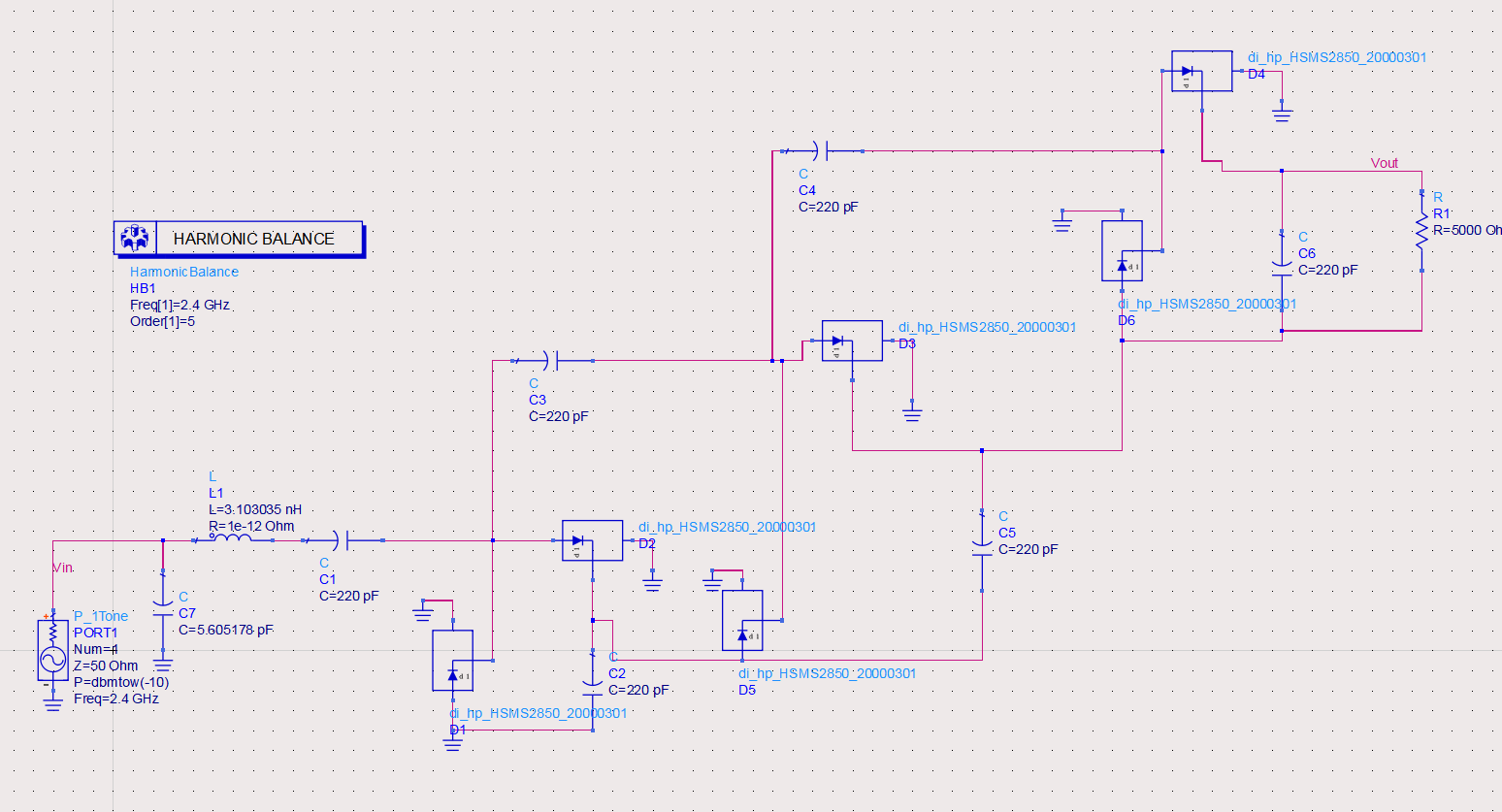
This has been asked by other students working on the same topic many times before: It is not possible because you have zero layout information in your design.
If you want to do the layout in ADS, you need to use components model with associated footprints. This can be a component library like Murata, or components from palette "Lumped-With Artwork".
Or use any other PCB package, the circuit is trivial enough and interconnect routing must be done manually anyway.
Thanks sir for your reply,
what do you mean by other PCB package ? do you mean other software like eagle,kicad...etc ?
also is it possible to make the layout manually by putting transmission line between each lumped component or it's useless ?
Are you sure that you will able to find HSMS2850 Schottky Detector Diodes ? They are obsolete coming form HP days..
Yes
Yes, that is the RF engineer's use of ADS, to include these elements in simulation (!) to see their effect on simulation results (!) and then create that (!) layout.
Thanks for you concern sir, but i have them already
so what should i do now is include TL and see the results on ADS then i move to another PCB software to be able to make the gerber file.