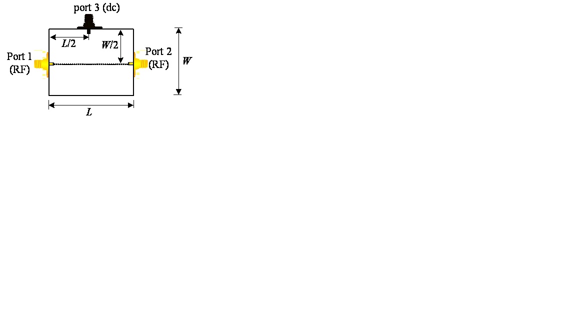
help me design a RF Choke on PCB
时间:04-05
整理:3721RD
点击:
Design an RF choke with the following specifications. You can use lump, distributed, or hybrid match configurations. The load elements are provided by teachers and all other components, SMA connectors, substrate, etching, soldering, and other expenditures are prepared by students.
Frequency Range: 2.3-2.7 GHz
(1) Return Loss (S11, S22) ≥ 28 dB
(2) Isolation (S21, S31) ≥ 28 dB
(3) Insertion Loss (S21) < 0.4 dB
(4) Circuit Profile and Size (W*H) ≤ 1.5*1.5 cm*cm
Please help i want have ADS Circuit Simulation thank u
Frequency Range: 2.3-2.7 GHz
(1) Return Loss (S11, S22) ≥ 28 dB
(2) Isolation (S21, S31) ≥ 28 dB
(3) Insertion Loss (S21) < 0.4 dB
(4) Circuit Profile and Size (W*H) ≤ 1.5*1.5 cm*cm

Please help i want have ADS Circuit Simulation thank u
A good choke at 2.4 GHz is simply a very thin line with a high impedance (>500 Ohms) compared to 50 Ohms. If you have room, you can make a meander line having even higher impedance. Make sure it will be well DC-conductive under the nominal DC current, and cannot get broken due to corrosion after some time.
so how can i desgn
There is nothing to "design". Simply run a thin line where you need.
