50 ohm buffer 10MHz to 40 MHz (wafer probe)
I want to design a 50 ohm buffer in frequency range 10MHz-40MHz which will be followed by wafer probes and then instruments. The baseband output of a receiver will be buffered.
I am planning for PMOS source follower with
a) current source load
b) resistive load
PMOS for low flicker noise. Which one is better a) or b).
Any other suggestion? I have no power limit. I need low noise.
What are your specs for output power? Distortion vs f, Noise level? I would stick with bipolar complementary drive with negative feedback and series 50R.
http://www.ti.com/lsds/ti/amplifiers...ramCriteria=no
If your requirement needs Low Noise, I suggest you to use Bipolar transistor at those frequencies if available.
Otherwise CMOS may be trouble..
Hi SunnySkyguy & BigBoss,
Thank you very much for your suggestions! I am using PMOS due to time constraints.
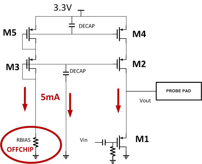
I have attached the circuit. i am using 3.3V I/O PMOS devices in 65nm process. The bias current is 5mA.
1. Is the current too high?
2. gm of M1 =1/Rload=1/50 (for S11=-15dB)
Gain=gm*Rload/(1+gm*Rload)=0.5
Is there a way to increase gain without matching circuit?
3. The sizes are
(w/l)1=600u/400n
(w/l)2,3,4,5=400u/400n
Is it ok to have different length devices in current source & M1? I am worried since thresholds may not track each other.
Is the design OK?

