Effect of buffer flicker noise in Voltage controlled oscillators
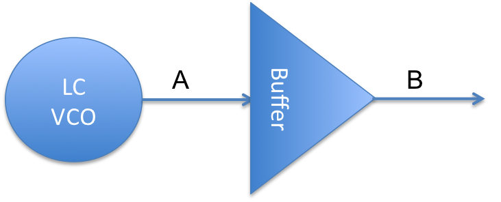
This is second post on this forum. I am trying to understand contribution of buffer in the phase noise of LC VCO in any CMOS process especially at the low offset frequencies (1/f3 region).
When one adds a buffer with the VCO core and simulate phase noise at both VCO output and the buffer output, the phase noise at the far offsets starts degrading at the buffer output compared with VCO output. The only way to recover the performance is to burn more current in the buffer.
Things become more interesting when we look at the behavior in the 1/f3 region. First of all, in the deep scaled CMOS processes, the buffer seems to contribute considerable amount of phase noise at low offset frequencies. Confusing part is even if the phase noise is probed at the output of VCO (and not at the buffer output) the buffer contribution is present there (from the noise contribution summary table). Assumption is, there is no feedback path between the output and the input of buffer. How does the flicker noise of buffer upconvert to carrier and appear at the VCO as well as buffer output? Any insight?
Even the fastest digital circuits operate in a linear region while changing state, and an essentially linear buffer amplifier should be linear all the way.
Phase noise (jitter) is just random modulation of the zero crossing point while passing through the linear region, caused by the addition of noise added on top of the signal.
Low frequency flicker noise also does this, and effectively frequency modulates the carrier. The more stages of amplification you add, the worse it gets.
Even though the bulk of the disturbing noise energy may be at a low frequency, it still frequency modulates the carrier at what may be running at a very high frequency.
The key word is "modulates" it does not just add.
And the modulation process produces some new frequencies which appear as close in phase noise sidebands either side of the original carrier.
Thank you for your reply. I think I should have explained better.
I am familiar with the phase noise up conversion mechanisms as discussed by J.J. Rael in his famous "Physical Processes of phase noise in differential LC oscillator". I also read recent works in ISSC and JSSC about noise optimization in 1/f^3 region of LC VCOs, in them, by recognizing Groszkowski effect in the up conversion of flicker noise, people proposed higher order tank with resistive impedances at not only fundamental frequency but also at second and third harmonic of oscillation frequencies.
So my confusion is following: in the attached figure

I really do not know the answer.
But usually a buffer is very loosely coupled to the oscillator to do what it has to do. Typically a small geometry junction FET is used for buffering with very low gate capacitance, not a mosfet.
However.... smaller geometry implies greater current density which in itself is bad from the point of flicker noise. So you may have two effects at work here working in opposite directions.
you are assuming that the buffer amp does not reflect any power, when in fact if reflects power and can even send spurious signals out of the input port. Put a 3 dB pad between the two and the effect will be much reduced.
