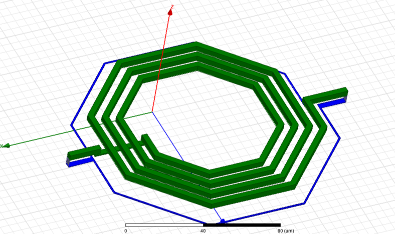
Why ground-ring of spiral inductor is narrow in PDK
The L is close with data of PDK, but Q factor is very low compared with PDk.
I think the narrow is reason why Q factor is low, but as you see, ground ring indeed is narrow.
I think ground ring as current return path should not be high impedance.
Anyone can help me?
BTW, how to export PGS(pattern ground shield) from cell in virtuoso?
Thanks

What type of conductor you have used for guard ring ?And why you have used a guard ring ? What is its purpose ?
How you have simulated Q factor, which set-up you have used ?Two port s-parameters or one port is short circuited ?
You have to mention some details...
Thanks
I export gdsII of inductor from virtuoso. the guard ring is M1 of tsmcN65 1p9m process. I think the guarding ring may be used as current return path in this way it connects two ports. As you know there are always guard ring in PDK like tsmc. I using two port s-parameter, calculate L and Q as follow
L:
im(1/Yt(port1_T1,port1_T1))/(2*pi*freq)*1e9
Q:
-(im(Yt(port1_T1,port1_T1))/re(Yt(port1_T1,port1_T1)))
I think my setup is same with HFSS help excepting I use M1 for ground ring but HFss help using pec(perfect conductor)
Based on many years of experience in RFIC inductor EM modelling, I really don't think this M1 ring should be your ground return. It makes no sense for multiple reasons:
1. Any closed ring around the inductor that is so very very close will reduce L and Q, due to induced current. Results are only useful if the circuit will have the exact same configuration and current flow (usually not the case).
2. The issue in item 1 is true even if the ground ring is not the return path, and only an unconnected ring around the inductor (mutual inductance). If the ground ring is the return path for EM simulation, it will change results even more. And we can't separate the inductor itself from the return path effects. We always get the total results of inductor with all return current through this simulated return path.
2. If we understand items 1 and 2, and still want that ground ring as return path, we would minimize the self-inductance and resistance of the ground return path.
In your case, the total resiatance is dominated by the ground return path. That makes no sense at all. I am sure that this M1 metal was not intended as the return path for the inductor. You need to create another configuration where you reference the ports to another ground (usually global ground at the bottom of the substrate, but HFSS can't do this well because it lacks accurate port calibration) or define a meaningful ground return path as it also exists in your circuit.
I very appreciate your reply.
The M1 ring is not closed but cut in one terminal. Do you think what the M1 ring is for?
perfect E boundary in bottom of Sub is used for ground in spiralinductor.pdf, I do the same to verify PDK inductor.
And connect spiral ring with ground ( bottom of Sub ) using pec. But the simulatin results is not right, L too high, Q too low.
Can you tell me how to connect spiral and ring with ground?
Thanks very much
I think the current density in sub and around pec connection to ground.
But I don't know how to eleminate this effection.
I don't know. In other PDKs, there is no such M1 ring. My only guess is that it illustrates a keepout area. What does the PDK documentation say?
Yes, your model is rather different from what was measured. It is really difficult to model this properly with HFSS, because the return path results will always be part of results. I very much prefer ADS Momentum or Sonnet for this type of work, because then you place the port references at the PEC at the bottom of the substrate (no M1 ground ring needed) and the solvers will accurately de-embeed the port parasitics. For HFSS there is no accurate way to de-embed the ports, and that's what causes real trouble here.
I think the PDK documention shows the inductor without return path. So don't use the m1 ground ring. Instead, connect your ports to the PEC at the backside of the silicon. You will then need to manually de-embed the parasitics of the ports, and that's a real challenge. In all documents from Ansys that I have seen on this topic, there was no real solution for this. They always tried to re-define the geometry to please the solver, and ignored that it's different from the measured setup.
I think this guardring ( or whatsoever) must be connected to global ground by ideal conductor vias otherwise it doens't make sense to lay down this guardring.
The guardrings are essentially used to protect the underlayer of a passive or active device on the silicon from noise,eddy currents etc.And they collect these magnetic and electrical fields to drain away to the GND and they should therefore be grounded.
Guardrings usually look different, and they are closed loops. Only as a closed loop, they can collect magentic fields. But of course, collecting magnetic field with a closed loop near the inductors means: it acts as a transformer with a shorted turns, reducing the L and Q of the inductor. So that type of configuration requires careful tradeoff.
In measurements, we often have such a closed loop, but at some distance. Why? For the N.5 turn inductors, where the terminals are on opposite sides, we do need some return path. Now the question is what to do with the inductance and resistance of that return path: include it in results or de-embed?
What I have seen is that the self inductance and resistance of the return path are usually de-embedded (not part of PDK electrical model) because the ground path from measurement is not included in the PDK layout, and the ground path will be different in the user's layout. What is usually not removed is the mutual inductance effect between the inductor and the ground frame, simply because there is no easy way to de-embed that. If the distance is sufficiently large, that error is small.


Hi volker@muehlhaus and BigBoss
You help me much.
Do you mean the GND at bottom of substrate by saying " mutual inductance effect between the inductor and the ground frame"?
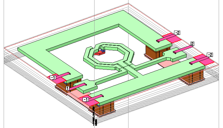
I see you are using Sonnet, but what do you think of using lumped port in HFSS to de-embed following attaching picture ?
With "ground frame" I mean any metal that is drawn on the top of the chip. This is what we have in measurements, and it is part of measured (raw) results. Usually there is some de-embedding top remove it from measurement results.
Mutual inductance refers to the coupling between inductor and that ground frame.
This is bad for multiple reasons. First, that user created PEC bridge will be part of results, which is bad. And for this example that you showed, we need some connection between the ground pads, otherwise no return current can flow. This seems to be done with vias in this example, which will also be part of the results. Overall you will get some results, but it's the inductor plus many other unknown influences. Not very useful.
- Using spiral inductor after SRF
- [ADS] Spiral inductor with SRF below the operating frequency
- [ADS] Spiral inductor parameterization in ADS
- How to calculate Q factor of square spiral coil on substrate?
- log spiral antenna in CST
- In RFIC, spiral inductor behaves as capacitor at some hight frequency . Why so?
