Matching impedance of input impedance
The amplifier below is operating at 1GHz ( fs = 1GHz).
As indicated in the circuit below, design a matching network (MN) circuit using a Smith Chart to match the source to the input impedance of the amplifier (ZL) for maximum power delivery.
Note you will need to consider the high frequency model for the transistor.
BFQ65 it will not work properly at 3V Vcc. All the parameters in the datasheet are given at VCE=8V.
For a 3V Vcc you have to choose a transistor heaving the performances measured at VCE about 2V, as the transistor below:
http://www.nxp.com/documents/data_sheet/BFG403W.pdf
The question is given like that. I am not suppose to deviate from it. Is there any way I can determine the input impedance using the high frequency model and also by that using the smith chart to determine the matching impedance.
Ok.
BFQ65 it will not work AT ALL at 3V Vcc. What you are going to do now?
It should work but the parameters will be very different to those given in the data sheet.
Time to fire up the VNA and dig thru the box of expensive test fixtures for one suitable for testing that part at 3V......
A couple of hints, Lc is going to have a high AC impedance at 1GHz (At least in theory, a real one may well have a self resonance issues up there).
Ce is going to be pretty much a short circuit at 1GHz (In theory, I wouldn't count on it in practise).
The match is clearly going to be an L match of some form, series L, shunt C in all probability (so that the biasing arrangements work).
You do not however have sufficient information to design the matching network, specifically you do not know the required bandwidth.
This should all be in your text book and lecture notes, going to the internet is a very poor second to going and talking to your tutor.
Regards, Dan.
If no specification is given in the exercise problem, I would expect smallband matching, the most simple LC or CLC low-pass network that achieves matching at 1 GHz.
Similarly the 8 V S-parameters will be considered valid for 3V (athough they aren't).
The tutor is not really helpful. I am not given the bandwidth. In fact, I am also asked to find the matching network parameters: bandwidth, gain and quality factor Q.
That is why I am having a headache about this. I do not have any headstart in this.
Your tutor have/must to understand that somewhere is a misunderstanding, and you have to choose different transistor for this application, if need to be supplied at 3V.
Do your homework and if you know how to show him your point of view he will understand.
For BFG403W (which I mentioned above and which is still in production) NXP provides all the models you need (S-parameters and Spice):
http://www.nxp.com/download/pip/BFG403W/models
Start first with the S-parameters and do the input/output matching, and later use the matching values that you got and use them with the nonlinear model (Spice) for fine tuning.
In the nonlinear model have to set the bias of the transistor the same as the bias specified in the S-parameter file that you used (e.g. 3V and 5mA).
My tutor does not even help. This is tough.
Is there any where that I can refer to any examples for help?
I have done something, however, am not sure whether is this correct after I have done matching.
Before
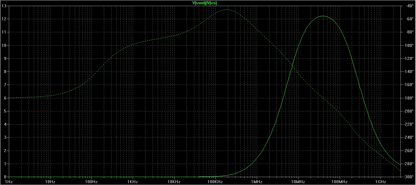
After

This is matched at 1GHz. Please take a look at around 1GHz. Hope that this is more or less correct.
The low gain at 1 GHz is further reduced in the second case. So the circuit is surely not impedance matched at 1 GHz.
At 1 GHz I think you can use some of the parameters of the datasheet, specially r_base, r_ex and r_c, which won't depend that strong on VCE, but much more on I_c and frequency, which in your case is quite low. You can also use the measured transistor capacitances from the datasheet (which are typically measured at 0V and 2 or 3 voltages more) and use a simple junction-capacitance model to find the required capacitances @ 3V. Once you got them, you can build a simple high-frequency hybrid-pi model of your transistor, which will be basically the input of an emitter-degenerated transistor because C_e is a short and L_c act as an RFC. Then you calculate the input impedance of your 50-Ohm loaded amplifier and can therefore design the matching section.
Hope that helps.
MK